Multilayer PCB Prototype Manufacturer China,impedance control HDI
Contract manufacturing of multilayer pcb, blind/buried via,Mass Production
Multilayre PCB, High speed,Shenzhen,China/USA/UK/India/South Africa
multilayer pcb is useful in high-speed application
-
multilayer pcb is used very normal.
The multilayer pcb is mainly used in industry electronic equipment,Like computers and military equipment, especially in the case that need light weight and volume.The multilayer pcb is also useful in high-speed application. The mltilayer pcb can provide more space for the conductor pattern and power.
Multilayer PCB |
|
Multilayer PCB Prototype |
| blind via |
|
Manufacturer China,impedance control HDI |
| HDI PCB |
|
blind/buried via,Mass Production |
Multilayer PCB |
|
blind/buried via,Mass Production |
| HDI PCB |
|
impedance control HDI |
| blind via |
|
Medical equipment aplication |
HDI PCB |
|
impedance control HDI |
| impedance |
|
0.1mm Laser drill via |
| Laser drill |
|
Multilayer PCB Fabrication |
Multilayer PCB |
|
Multilayer PCB Fabrication |
| impedance |
|
Multilayer PCB Prototype |
| Laser drill |
|
Carbon/Silver Ink Printing or Gold-plated Surface |
impedance |
|
Multilayer PCB Fabrication |
| Multilayer PCB |
|
Multilayer PCB Prototype |
| Aplication: |
|
Industry control boards |
Benefits of Multilayer PCBs
-
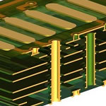
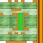
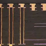
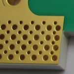
The multilayer pcb is made up by more than two layers which are stacked together with reliable through via or blind via between them. There are at least three conductive layers in one multilayer pcb with two layers outside and the one layer inside the PCB. Due to the complex manufacturing process and lower production , the cost of multilayer pcb is relatively higher.PCBSINO is specialized in multilayer PCB manufacturing for many years.
Benefits of Multilayer PCBs
Benefits of Multilayer PCBs (compared to single or double-sided PCBs)
Higher assembly density
Smaller size (considerable savings on space)
Increased flexibility
Easier incorporation controlled impedance features. EMI shielding through careful placement of power and ground layers.
Reduces the need for interconnection wiring harnesses (reduces overall weight)
multilayer PCB fabrication – lay-up and bond
The outer layers of our multilayer consist of sheets of glass cloth pre-impregnated with uncured epoxy resin (prepreg) and a thin copper foil.
Multilayer PCB
Multilayer PCBs have one or more conductor pattern inside the board, to increase the area available for the wiring. This is achieved by gluing (PP) many double-sided circuit boards together with insulating layers in between.
The number of layers is referred to as the number of separate conductor patterns – usually including the two outer layers. Most boards have between 4 and 8 layers, but PCBs with almost 100 layers can be made.
Since the layers in a PCB are laminated together, it’s very difficult to tell how many there are, but if you inspect the side of the board with magnifier closely you might be able to count them.
Large super computers often contain boards with multilayer PCB.
Applications of Multilayer PCBs
-
Applications of Multilayer PCBs
While the weight and space benefits of multilayer PCBs are especially valuable for Aerospace PCBs, multilayer PCBs are also apply to many critical product. below are a few other the applications using multilayer printed circuit boards:
Computers
File servers
Data storage
Signal transmission
Cell phone transmission
Cell phone repeaters
GPS technology
Industrial controls
Satellite systems
Hand held devices
Test equipment
X-ray equipment
Heart monitors
Cat scan technology
Atomic accelerators
Central fire alarm systems
Fiber optic receptors
Nuclear detection systems
Space probe equipment
Weather analysis
For furhter information, please feel free to contact us, www.pcbsino.com
 English
 Español
 Português
 Deutsch
 Français
 Italiano
 Россия
 Türkçe
 Polski
 Suid-Afrika
 بالعربية
 فارسی
فارسی