Aerospace Rogers PCB aplication
China PCB Manufacturing, Shenzhen PCB Manufacturer, Making Circuit boards
PCB Contract manufacturer, PCB Fabrication, Turnkey assembly services
Buy Print circuit board, customer: /USA/UK/Canada/South Africa...
PCB Supplier Shenzhen, China, PCB Manufacturer, Turnkey services
-
PCBSINO is the Top 5 PCB manufacturer company in China.
PCBSINO do rapid Prototype within 24 hours. our rigid PCB like MCPCB and Rogers PCB, FR4, High TG FR4, Rogers 4003, 4350,Al Aluminum metal Core MCPCB, Al2O3 Ceramic,Taconic,Halogen Free material, CEM-3, Fr2, CEM-1, CEM-2, 94VO, Rogers HF material, Polymide, etc.
PCBSINO making many type electronic product for our customer, Our turkey services team can source original components part for your project(Digikey/Mouser/RS...), senior Electronic engineer will follow each step of the production to solve any PCB problem and our team will do final function test in PCB house.
Express PCB |
|
Rigid PCB Rapid Prototype,24 hours |
| Fr4 PCB |
|
prototype Lower to 15USD ! |
| Rapid Prototype |
|
Fr4 Rigid PCB Rapid Prototype China, |
MCPCB |
|
MCPCB Manufacturer China, Shenzhen |
| Aluminum PCB: |
|
Aluminum Metal Core PCB manufacturing, Fabrication |
| Aluminum PCB: |
|
single side, double side MCPCB, 0.5-5mm or more |
Rogers 4350B |
|
Rogers 4350,Rogers 4003 Manufacturing |
| Rogers 4350B |
|
Rogers 4350B,4003C PCB Manufacturer |
| Ro4350B |
|
Rogers High Frequency PCB Manufaturing China |
Turnkey Services |
|
Turnkey PCB Assembly Services, |
| Turnkey services |
|
Print circuit board Manufacturing, Turnkey Services |
| Turnkey Assembly |
|
Through Hole PCB components wave soldering Assembly |
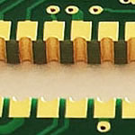
Aerospace Rogers PCB aplication
-
Aerospace Rogers PCB aplication
This is a type of Rogers PCB material, which is non-brominated. This material comes in different configurations and uses the glass fabric styles of 1674 and 1080 that meet the electrical performance specifications of the same laminate. This material is mainly used in:
High Frequency PCB are widely used in wireless networks, wireless communications and satellite communications, in particular the popularity of 3G/4G/5G networks exacerbate the market demand for the product on the HF PCB. For some special high-frequency PCB materials ( such as: Teflon PCB material, Rogers PCB material ), we have sufficient inventory.
Gold is highly touted as a plating material for conductors and electrical contacts. It exhibits high conductivity, at 4.52 × 10⁷ S/m, although this is less than the conductivity of copper, at 5.817 × 10⁷ S/m. Silver actually has higher conductivity than copper, at 6.301 × 10⁷ S/m. Plated finishes applied with silver tend to be extremely thin, so the benefits of such high conductivity typically won’t be seen at lower frequencies. However, at higher frequencies, with very thin skin depth, the effects of having a plated finish with conductivity that is higher than copper may be more noticeable.
The impact of final surface finish on circuit loss will depend not only on the type of surface finish but on the thickness of the substrate material and the type of transmission-line technology, such as microstrip or grounded coplanar waveguide (GCPW). In a microstrip circuit, with its configuration of dielectric material between a bottom layer ground plane and top-layer signal conductor, the electric (E) and magnetic (H) fields form high current density at the edges of the microstrip transmission line. For a circuit that is plated with a material having less conductivity than copper, such as electroless nickel immersion gold (ENIG), the high current density at the edges of the transmission lines will use the plated finish more than the copper beneath, resulting in higher conductive loss than when using pure copper.
In the case of copper plated with ENIG, the losses are frequency dependent, increasing at higher frequencies. The frequency dependence is caused by the way that current uses a conductor differently at different frequencies—the so-called “skin effect.” At lower frequencies, the current uses more of the full cross section of the conductor. At higher frequencies, the current flows only along the outside or the skin of the conductor. As the frequency of a microstrip transmission line increases, the current flows through less of the copper conductor and more of whatever plated finish is on that conductor.
Following are some types introduction for Rigid PCB and High Frequency PCB:
FR4 PCB(2layer,4 layer,multilayer)
Rogers(RO4003,RO4350,RO5880,RO3003,RO3010,RO3206,RO3035,RO6010)
F4B high frequency pcb board
Taconic(TLX-8,TLX-9,TLC-32,TLY-5,RF-60A,CER-10,RF-30,TLA-35)
Arlon high frequency pcb board
ISOLA high frequency pcb board
At the same time, we also provide corresponding PCBA services as our customer’s design and requirement.
Castle Microwave can provide a wide range of innovative and class leading components suited for the aerospace sectors. Ranging from broadband Antennas, to positioners, cable assemblies and safety systems.
Our Experience ranges from component supply to consultation and testing of avionics and mission critical systems.
Sufficient stock:
We have sufficient rogers material raw as follow:RO4003C、RO4350B、RO4360、RO4533、RO4535、RO4730、
RO4232、RO4233、RO3003、RO3006、RO3010、RO3035、RO3203、RO3206、
RO3210、RO3730、RO5780、RO5880、RO6002、RO3202、RO6006,
Frequently-used is 4003C,4350B,5880
So we can do pcb circuit board with your detail requirements in the case of you send us gerber files or any other files
Rogers Is a plate, the material is characterized by a superior dielectric
electronics high frequency circuit
constant temperature stability, dielectric constant thermal expansion coefficient
and copper foil is very consistent, to improve the PTFE substrate.
This product is ideal for applications where the ambient temperature
is rapidly changing (aerospace) and can be used for higher frequency
and multilayer structure due to its low dielectric loss and high reliability of metallized vias
Company Service:
24 hours quick sample is avaliable here.
reply Customer's any enquiry within 3 hours;
Blind buried hole ,crossed blind hole can be done
24 hours Engineering Gerber files treatment.
24 hours English Engineering Questions Confirmation by E-mail.
Supply the best project fit for production customized
Sincerely look forward to cooperating with you.
If you have a product quotation, please do not hesitate to contact us, thank you!
For a microstrip line with ENIG finish, the current will use different combinations of the three conductive metals, depending upon frequency. At lower RF, all three of the conductive metals contribute to current flow. At higher RF or lower microwave frequencies, the current flow takes place more through the nickel and gold. And at higher microwave frequencies or lower millimeter-wave frequencies, where the current density is more concentrated around the edges of a microstrip line, current uses more of the gold as a conductor, with the conductivity characteristics of the gold contributing more to the final conductor-loss performance than at lower frequencies.
The type of circuit layout and transmission-line technology can also play a hand in how the choice of a plated finish translates into the conductor loss of a high-frequency circuit. For microstrip transmission lines, where the current density is high around the edges of the conductor, some loss will occur because of the skin effects at higher frequencies. But in a circuit configuration like GCPW, in which the two waveguide-like transmission lines each have two edges, for a total of four edges, the current density will be high at those four edges of the circuit. As a result, for a GCPW circuit with its four conductor edges, a plated finish will have a greater impact on high-frequency loss than for a microstrip circuit with its two edges.
A dielectric material is a substance that is a poor conductor of electricity, and used as an insulating layer in the PCB build up. Porcelain, mica, glass, plastics and some metal oxides are good dielectrics. The lower the dielectric loss, (the proportion of energy lost as heat) the more effective the dielectric material. If the voltage across a dielectric material becomes too great -- that is, if the electrostatic field becomes too intense -- the material will suddenly begin to conduct current. This phenomenon is called dielectric breakdown. Taconic offers several materials that are less likely to demonstrate a dielectric breakdown condition than FR-4.
Pre-impregnated (Pre-preg)
Contraction of 'pre-impregnated composite fibers', and in the manufacture of PCBs, pre-pregs help influence the performance characteristics of the printed circuit board.
A term also used in the PCB fabrication industry to describe the bonding ply materials used to bond the layers of a multilayer PCB together.
You can get more information on all of Taconic's laminate products from their website
As a way of demonstrating these differences in surface-finish conductivity for different transmission-line circuits, broadband measurements were performed on equivalent-length circuits with microstrip and GCPW, each fabricated on two versions of 8-mil-thick RO4003C™ circuit laminates from Rogers Corp., one version with bare copper conductor and the other with ENIG finish. Broadband measurements were made on all four circuits from 10 MHz to 50 GHz with a commercial vector network analyzer (VNA). Significant differences were found between the ENIG finished and bare-copper circuits for both circuit types, although with greater losses exhibited for the GCPW circuit with ENIG finish
Large panel capability
Embedded capacitance and resistance
High density wireability options utilizing thin dielectrics/narrow linewidths, integrated HDI technology, and large drill aspect ratios
Plating aspect ratios up to 22:1
Quickturn PCB fabrication for significant cycle time reductions
Wide variety of materials from trusted suppliers including Panasonic, Park, Rogers, Isola, Dupont and many more
A wide variety of surface finishes from OSPs to multiple metal surface finishes (including SnPb, Pd, ENIG, ENIPEG, and Ag)
For mission-critical applications in defense and aerospace, high performance super computing, industrial or medical, i3 PCBs are the complete solution.
Wearables and today’s associated technologies are gaining greater traction. Everywhere you turn, there’s a new wearable device with applications ranging from health and fitness monitoring onto advanced pain relieving devices, and there are more on the way in all shapes and sizes.
When dealing with a wearable PCB design, a number of factors have to be taken into consideration. Among the areas that demand close attention are board surface materials, RF/microwave design, and RF transmission lines.
They are also used for structural, vibration and flight testing of aircraft, as well as satellites for vibration, pyroshock, force limited vibration and acoustic stress testing. They can also be used in wind tunnels and to measure aircraft noise.
PCB® products are used for applications such as explosive, gun and small arms ammunition testing, fuze or safe and arm of ammunition systems, penetration shock recorders, and impact testing.
PCB® also has extensive experience with underwater vibration and unsteady, rapidly fluctuating pressure and cavitation measurements.
Fig 1 – Stack Up FR4 & Rogers
FR4 material has been around forever with excellent performance. Everybody knows about it and is well known in PCB design circles. But now, some wearable devices are calling for more advanced Rogers’ materials. So, it’s best to understand a wearable PCB design requirements before assuming FR4 is ok to use.
In some wearable PCB applications, a combination of FR4 and Rogers’ material can be used as shown in the stack up, Fig. 1.
Also, RF/microwave design, once solely in the high-end mil/aero domain, has migrated to the consumer wearable sector. Now, the PCB designer working on wearables is tasked with this more challenging design aspect, plus getting a better handle on the right PCB materials.
Microwave/RF Applications
Defense and Aerospace Applications
Radio frequency (RF) refers to the 500 MHz to 2 GHz frequency bandwidth. It has come represent signals sent at high frequency over a controlled impedance line, using ground or shielding to prevent signal degradation. Coaxial cable is an example of a more generic definition where RF is carrying the current to wires. It becomes a transmission line with electromagnetic fields. The result of the fields is of minor importance at lower frequencies, but at higher frequencies it becomes significantly important. These fields and related effects such as return loss, VSWR (Voltage Standing Wave Ratio), and insertion loss are important when designing for robustness.
Connectors are critical to a successful transmission line because they must perform the mating segment or assignment without degradation of the signal itself.
For separate RF connections it’s even more important. When matching circuitry impedances, it is vital to make sure that when the signal goes to the power supply outside the PCB, minimal signal loss is being incurred by using the non-performing RF cable or shield.
Transmission signal length is important to avoid a mismatch between the transmission and reception. If there’s a mismatch, it’s going to create a nonbalanced return signal, which bounces back to the lines, produces an inbound wave, and may create waveform distortion, degrading the signal.
If the mismatch is high, the incoming signal will be lost because the return signal is so strong it cancels it completely. For RF applications, transmission and return lines must be equal. They need to be as short as possible, and go from point A to point B without many curves or bends. The RF signal needs to be shielded properly because they are frequency sensitive. It’s easy to create a ripple effect or bounce back, or skin effect. Ground bounce is generated to create undesirable noise or cross-talk, thereby reducing transmitting signal strength.
EPC manufactures printed circuit boards, specializing in proto type to medium volume requirements with a focus on high reliability circuitry for the Military, Aerospace, Space Exploration and Satellite Systems. We manufacture Rigid and RF Circuit Boards. These parts are primarily used for radar and missile systems, antennas, communications, aircraft control, test equipment and power amplifiers.
Our key customers are some of the largest mil-aero prime contractors in the world. We serve Ball Aerospace, Lockheed, Raytheon, Harris, Orbital Sciences, BAE Systems, General Dynamics, General Atomics, NASA Goddard, and many of their subcontractors across the country.
These are extremely demanding customers with critical reliability needs. The foundation of our business is to provide our customers the most reliable circuit boards that can be made, and supply extraordinary service through the review, quotation and order fulfillment process. Our service and communication have resulted in being the preferred supplier for many of these high-rel applications.
PTFE is used as non-stick coating for commercial applications due to its inert molecular structure. Its surface can be “roughened” only through drastic measures. PTFE/woven glass base materials are not surrounded by the myth of something exotic anymore. Asecured manufacturing and defined processing to pcbs are the guarantors for it. Rapid growth ofapplications operating at high frequencies demands a material availability with proven performance over many years. These facts are both given with PTFE/woven glass base materials.
In Rogers’ Advanced Circuit Materials Division, they manufacture high frequency laminates for applications in the wireless base station, aerospace and defense, automotive, high-speed digital and advanced chip packaging industries. All of products are manufactured in an ISO-9001:2008 certified facility with “ahead of the curve” process technology.
Responsible for purchasing all commodities for sensors in aerospace and military applications.
Trained junior buyers to purchase Electronic parts.
Purchase parts from Domestic and International sources to secure best price and delivery.
Confident making decisions and taking action based on material or specification requirements.
Complete understanding of MRP and what drives demand via BOM structure down to component levels.
Worked on team to Implemented new ERP system Y 2009.
Involved in BOM review and ECO process, sign-off for ECO related to purchasing issues.
Part of MRB team with Quality to determine disposition of material.
Daily communications with Engineering, Sales, Quality, and Accounting to resolve a multitude of issues.
Countersink Hole PCB
A countersink is a conical hole cut into a manufactured object, or the cutter used to cut such a hole. A common use is to allow the head of a countersunk bolt or screw, when placed in the hole, to sit flush with or below the surface of the surrounding material.
We specialize in Quick turn PCB services with an industry leading turnaround time as fast as 24 hours. When your company needs fast and rapid PCB prototyping, you can count on Custom Circuit Boards to deliver high quality printed circuit boards on time with competitive pricing.
PCB prototypes.
Philip Johnston, Trackwise Managing Director, commented “We are delighted with the results of recent trials. Whether or not this is the largest multilayer printed circuit ever manufactured – the next phase will see Trackwise manufacture a 25metre/80foot multilayer PCB – this is clear demonstration of the core offering of Improved Harness Technology™ - length-unlimited multilayer printed circuits to replace conventional wire harness or EWIS.”
Improved Harness Technology™ is a patented, proprietary technology that brings, for the first time, the proven benefits of flexible printed circuits – weight saving, space saving, improved precision, improved reliability – to system level applications.
Perfect for testing or one-offs, utilize our entry-level prototype PCB services with up to 500 boards completed in a few days. With our extensive prototype PCB fabrication capabilities, we are confident that we will exceed your company's expectations for all of your simple to complex PCB prototype requirements.
Peelable Solder Mas
Peelable Solder Masks (also known as strippable mask or blue-mask) are applied by screen-printing, act as in-process protection and are removed either after processing at the PCB manufacturer or at the assembler.
Peelable Solder Masks, provide such protection in soldering processes like wave soldering, reflow soldering or hot-air solder leveling (HASL). Reliable, time-saving and cost-saving in their application, they have long surpassed manual masking with heat-resistant tapes.
The last of those layers, substrate, is made of fiberglass and is also known as FR4, with the FR letters standing for "fire retardant." This substrate layer provides a solid foundation for PCBs, though the thickness can vary according to the uses of a given board.
A cheaper range of boards also exist on the market that don't utilize the same aforementioned PCB materials, but instead consist of phenolics or epoxies. Due to the thermal sensitivity of these boards, they tend to lose their lamination easily. These cheaper boards are often easy to identify by the smell they give off when being soldered.
PCB second layer is copper, which is laminated onto the substrate with a mixture of heat and adhesive. The copper layer is thin, and on some boards there are two such layers - one above and one below the substrate. PCBs with only one layer of copper tend to be used for cheaper electronics devices.
The massively-used copper clad laminate (CCL) can be classified into different categories according to different classification standards including reinforcing material, used resin adhesive, flammability, CCL performance. The brief classification of CCL is shown in the following table.
1 Layer Ceramics PCB
Ceramics PCB
Material: Al2O3 Ceramic Substrate
No of Layer: 1 layer
Board thickness: 1.6mm
Copper thickness: 1oz/35um
Surface finishing: Immersion Gold/ENIG
Solder mask: Taiyo white solder mask
In our production facilities in Dendermonde (BE) and Malville (FR), ACB employs 200 people and the two plants achieve an annual turnover of approximately 24 Mio Euro. We produce PCBs for a large and varied customer base, in the avionics, space & defence, telecommunications and medical industries, mainly in Western Europe.
Our strong focus on customer service and technical leadership, as well as the quality and on-time delivery of our high technology PCBs has allowed ACB to build and maintain our reputation as the most reliable PCB supplier in Europe.
Today, VARIOPRINT is one of the leading manufacturers of HF circuit boards for radar applications, as used in the automotive industry, for instance. Thanks to specially tuned processes, we can offer our customers maximum security in HF performance, especially in the range of 77 and 79 GHz applications
Rogers manufacture an extensive selection of high frequency laminates for a wide range of applications. Among these are materials with a range of dielectric constants, low dissipation factor,temperature stability, and controlled mechanical properties and some materials priced for low-cost commercial applications.
Taconic Advanced Dielectric Division manufactures PTFE/woven glass base materials for microwave, RF and high speed digital applications. Applications include LNAs, LNBs, PCS/PCN antennas, GSM and UMTS antennas, power amplifiers, filters, passive components, automotive cruise control, aerospace guidance telemetry, phase array radar, etc.
Rogers yog ib phaj, cov khoom siv thaum yog yus muaj ib dielectric superior
qhov kub stability, dielectric tsis tu ncua thermal expansion coefficient
thiab yog tooj liab ntawv nyiaj heev li, zoo qhov PTFE substrate.
Zoo tagnrho rau cov kev siv cov khoom no yog qhov uas tus kub ambient
yog mus pauv (aerospace) thiab yuav muab siv rau ntau zaus
thiab multilayer qauv vim nws cov dielectric uas tsis muaj hluav taws thiab muaj kev cia siab rau ntawm metallized vias
Daim ntawv thov:
ib Telecom: transmitter. Receiver. Oscillator. Kav hlau txais xov.
b Satellite receiver
lawv qhov chaw thoob ntiajteb no, amplifier, satellite telecom
d Microwave kis
e tsheb hauv xov tooj
f ntsuas apparatus, kws soj ntsuam kev LSI, analyser, teeb liab oscillator
g loj teletcom, kis tau tus mob kev kub ceev, siab ruaj, kis tau tus mob siab zoo, siab
nco
Circuit materials for RF/microwave applications are available from a wide range of quality suppliers, including Arlon, Isola, Panasonic PCB materials, Rogers Corp., and Taconic. All offer a variety of materials in a number of sheet sizes, with different dielectric constants.
Some, in fact, are developing environmentally friendly versions of PCB materials, such as RO4835HF halogen-free PCB materials from Rogers Corp. and Green Speed materials from Isola, which can be processed in the manner of low-cost FR4 circuit materials.
PTFE based materials are not included in any current or future regulatory guidelines or bans. The outstanding characteristics of PTFE including thermal stability, flame resistance, electrical properties and durability of electrical properties render this plastic as the top candidate for printed circuit boards.
For furhter information, please feel free to contact us, www.pcbsino.com