blind and buried via Multilayer PCB China, high speed pcb
Contract manufacturing blind via pcb, buried via pcb,laser drill 0.1mm via
blind and buried via HDI PCB,Shenzhen,China/USA/UK/India/South Africa
blind via |
|
blind and buried pcb, |
| buried via |
|
blind and buried via Multilayer PCB China, |
| HDI PCB |
|
high speed PCB |
blind via |
|
Contract manufacturing blind via pcb, |
| buried via |
|
blind and buried via Multilayer PCB China, |
| HDI PCB |
|
blind and buried pcb, |
blind via |
|
high speed PCB |
| buried via |
|
buried via pcb,laser drill 0.1mm via |
| High speed |
|
blind and buried via HDI PCB, |
Blind and buried via solution
-
Blind and buried via solution
When your design does not allow you to put enough PTH vias due to surface constrains, blind and buried vias might offer you a solution.
Blind and buried via
A. is a blind via drilled and plated through before pressing the multi layer. To produce this you will need to select the appropriate build up (reverse) and select an extra PTH run in the order details.
C. is also a blind via but laser drilled and plated after the multi layers has been pressed. That technology is not used by Eurocircuits.
B. is a buried via as he cannot be seen from outside. The via hole is drilled and plated before the pressing takes place. These holes will also represent an extra PTH run.
Blind and/or buried vias present in your data also need to be specified in your order details. This is done by selecting the appropriate build up in the buildup wizard and the correct number of extra PTH runs and extra press cycles that are applicable.
Define the blind/buried via either though the padstack editor or within the Allegro design using Setup >Vias > Define B/B Via or Setup > Vias >Auto Define B/B Via. Using the setup bb vias GUI you can copy the pad definition of an existing via, set the start and end layers. Using the Auto define GUI you select the input pad name, with an optional prefix, set the start and end layers, set the rule set(s) and generate the via.
Add the via(s) to the physical constraint set(s) if you didn't use the Auto define methodology.
When in add connect set the start (Active) and end (Alternate) ayers and select which via you want to use
Plating Through Hole(PTH)
Plating through hole is the most common via, just take up PCB and face to the light, if you can see the light, then it is the “through hole”. PTH is also the simplest kind of hole because it just need to use drill or laser light to make a full borehole, and the cost is relatively cheap. But some circuit layer do not need plating through hole. Although PTH is much cheaper, sometimes, it may use some more PCB space.
Blind Via Hole(BVH)
-
Blind Via Hole(BVH)
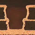
Connect the outermost circuit of the PCB and the adjacent inner layer with plated through-hole, since we cannot see the opposite, so it is called “blind pass”. In order to increase the space utilization of PCB circuit layer, blind via hole came into being. Please note that this production method requires special attention to the depth of the hole (Z axis) should be appropriate. Almost no PCB manufacturer adopt this kind of method because the difficult of hole plating.
Buried Via Hole (BVH)
Buried via hole connects to any circuit layer of PCB but do not pass to the outer layer. This process cannot be done using the method of bonding after drilling, it must be in the individual circuit layer when the implementation of drilling, the first part of the internal bonding after the first plating treatment, and finally all the bonding. Buried via hold need more time than the original “through-hole” and “Blind hole”, so its’ price also the most expensive. This process is usually used in high-density (HDI) circuit boards to increase the other circuit layer can be used space.
Blind/buried vs. through hole vias?
I'm trying to learn PCB design and, from what I've read and seen, there appear to be three different types of vias:
Through hole - goes all the way through the board
Blind - goes from the top or bottom layer to some layer in between the top and bottom, but not all the way through
Buried - is between the top and bottom layers
It seems like most semi-complex boards I've had the opportunity to look at are 4-layer boards, and that usually one layer is dedicated to GND, another to VCC, and then the other two have traces. My question is what kind of via is most appropriate when trying to connect a pad or trace from one layer to the GND or VCC layers? I ask because I would have thought that a blind or buried via should be used, but it seems like most boards I've looked at use through hole vias and that there's just a stop around the via on the layers it's not supposed to be connected to. Is there a reason to use that method instead of using a blind or buried via?
Difference between Blind and Buried vias?
blind vias are connecting a inner layer to either the top or bottom layer, and the other layer is blind as it doesn't see the via.
buried via is connecting two inner layers, without access to top or bottom layer.
that's different from the regular via that connect top layer to bottom layer and pass through all inner layers.You could have googled before posting this.
Blind vias are via holes which are formed to connect the outer circuit with inner layers, but DO NOT go through the entire board
Buried vias are via holes used to connect inner layers and are not visible in the outer layers.
In the case of multilayer boards (e.g. 4 layers)
Blind via = Via goes from one of the outer layers and does not appear the other side.
Buried via = via sandwiched between the outer layers and can not be seen.
BLIND AND BURIED VIAS advantages and disadvantages
-
BLIND AND BURIED VIAS advantages and disadvantages
Blind / Buried Vias
Definition
Blind Vias start on an outer layer but terminate on an inner layer; Buried Vias exist only between inner layers and do not begin or terminate on an outer layer.
Applications
Blind and buried vias are real estate savers because features and lines can be designed above or below (without making a connection).
Blind & Buried Via
When PCB space is limited, or you're working with tight plated through hole constraints, Blind and Buried Vias may be the answer.
Blind & Buried Via technology has played a pivotal role in squeezing more capability into a smaller space. By shortening vias to only pass through necessary layers, more surface area become available for components.
Key benefits include:
Ability to meet the density constraints of lines and pads on a typical design without increasing the layer count or board size
PCB aspect ratio reduction
Untitled-2Blind Via is a copper plated hole that connects only one outer layer to one or more inner layers. A blind via never goes all the way through a circuit board. In terms of design, blind vias are defined in a separate drill file.
Additional Benefit of Blind Vias:
Ability to widen BGA breakout channel (layer count reduction), Buried Via is a copper plated hole that connects two or more layers.
BLIND AND BURIED VIAS advantages and disadvantages
using blind and buried vias in a PCB design has its advantages and disadvantages. The advantage, of course is that this technology offers a viable design technique to help meet the density constraints of lines and pads on a typical design without increasing the layer count or board size. The disadvantage of the technology is that due to the additional operations in manufacturing the board, the cost of a board using blind and/or buried vias is significantly higher than a typical multilayer board with the same number of layers.
Designing a PCB with blind and buried vias is not that much different from using standard vias that go all the way through a board, and most designers with even moderate levels of layout experience will soon get a feel for it. The designer must be vigilant when it comes to the placement of the vias, perhaps more so than with conventional vias. Buried vias are easy, because they do not impact any trace or surface mount component on the top or bottom layers of the board. Remember that they are completely buried within the board. As long as the designer maintains the typical clearances from other pads or traces within the inner layers, they are really no different than conventional vias. Since they are completely buried, the designer can now place a trace or an SMD pad on the outer layers directly over the buried via, thereby gaining some added space on the outside layers. The placement of blind vias is not much different. Again, standard clearance rules apply. It is often tempting to place blind vias under SMD components to save just that extra bit of space, but this practice is not recommended. Solder flux has a nasty tendency to become trapped in the blind via hole, and although the flux is not highly corrosive, it can cause corrosion problems with time. This can cause hard to find and often mysterious failures of electronic equipment long after the assembled board passed all tests, even if the board has never been installed.
Reduce Your PCB Costs With Blind Vias, Buried Vias & Microvias
High Density Interconnect (HDI) circuit board designs have a higher wiring and pad density than conventional PCBs, along with smaller trace widths and spaces. They require advanced PCB technologies such as blind vias, buried vias, and microvias. HDI PCBs are usually more costly than conventional PCBs due to the complex build-up process involved in fabrication.
Although HDI PCB fabrication can be expensive, there are several situations where blind vias, buried vias, and microvias can offer a cost-effective solution. Here are just a few scenarios where advanced PCB technologies may actually reduce the overall manufacturing cost.
Blind and buried vias
Blind and buried vias are used to connect between layers of a PCB where space is at a premium. A blind via connects an outer layer to one or more inner layers but does not go through the entire board. A buried via connects two or more inner layers but does not go through to an outer layer.
BUT:
Not all combinations are possible. This is explained in this blog.
Blind and buried vias add considerably to the cost of a PCB. They should only be used when absolutely necessary. To help designers of tight boards, we offer via holes down to 0.15 mm in our pooling services and down to 0.10 mm as a non-poolable option. These need minimum outer layer pad sizes of 0.45 mm and 0.40 mm respectively.
Blind & Buried Vias
Due to the increasing complexity of design structures blind vias and buried vias are increasingly used in high-density circuit boards (HDI).
A blind Via connects exactly one outer layer with one or more inner layers.
A buried via is a via between at least two inner layers, which is not visible from the outer layers. This technology allows more functionality in less board space (packing density).
For furhter information, please feel free to contact us, www.pcbsino.com
 English
 Español
 Português
 Deutsch
 Français
 Italiano
 Россия
 Türkçe
 Polski
 Suid-Afrika
 بالعربية
 فارسی
فارسی