Pressing process of rigid-flex PCB Flex PCB application
China Flex PCB Manufacturing, Shenzhen Flex PCB Manufacturer, Making Flex Circuit boards
Flex PCB Contract manufacturer, PCB Fabrication, Turnkey assembly services
Buy Flexible Print circuit board, customer: /USA/UK/Canada/South Africa...
Flex PCB Supplier Shenzhen, China, Flex PCB Manufacturer, Turnkey services
-
PCBSINO is the Top 5 PCB manufacturer company in China.
PCBSINO do rapid Flexible PCB Prototype within. we can make Flexible Print circuit boards and Rigid circuit boards, Flex and Rigid Flex PCB, single side, double side, multilayer Flexible print circuit board
PCBSINO making many type electronic product for our customer, Our turkey services team can source original components part for your project(Digikey/Mouser/RS...), senior Electronic engineer will follow each step of the production to solve any PCB problem and our team will do final function test in PCB house.
Flex PCB |
|
Rigid FlexPCB Rapid Prototype |
| Flex PCB |
|
prototype of Flex PCB |
| Flex Prototype |
|
Rigid-Flex PCB Rapid Prototype China, |
Turnkey Services |
|
Turnkey Flex PCB Assembly Services, |
| PCB assembly |
|
Print circuit board Manufacturing, Turnkey assembly |
| PCBA Assembly |
|
SMT Assembly, EMS/OEM supplier China |
Pressing process of rigid-flex PCB Flex PCB application
-
Pressing process of rigid-flex PCB Flex PCB application
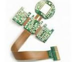
Production of a flex-rigid pcb
The production of rigid-flexible circuit boards varies depending on the construction.
The production of a 1F-1Ri construction serves as an example.
The manufacturing process is largely comparable with that for the production of a 4-layer multilayer. Differences are seen in the materials and the additional milling processes:
The rigid-flex PCB manufacturing process is time consuming and laborious when compared to traditional rigid board fabrication. It involves several steps that must be carried out with extreme accuracy. Mishandling or misplacing any of the flexible components in the board affects the efficiency and durability of the final assembly substantially.
Figure 2.4: Detailed Stack Diagram including plated-through holes for each flex section, as well as final through-plated holes in the rigid section (click to expand).
In the example stack up shown in Figure 2.4, we have two pre-etched and cut flex circuits, each double sided and plated through. The flex circuit has been blanked into a final assembly panel including boarders for framing – this will keep the flex circuit flat during final assembly after lamination with the rigid panel sections. There are certainly some potential hazards with inadequate support of flex circuit elbows and large open sections during assembly – especially in the heat of a reflow oven.
While this example does show adhesive layers it’s important to note that many designers are shying away from using adhesives, due to unacceptable z-axis expansion in reflow. However FR-4 pre-preg and thermosetting epoxies effectively achieve the desired result and are for all intents and purposes here considered ‘adhesive’ layers. Additional adhesion can be achieved through treatment of the copper on the flex layers to improve the ‘tooth’ into the laminated prepregs. Adhesive-less double-sided flex laminates are shown here. These are entirely polyimide film with a bondable polyimide coating which the copper foil is bonded to. DuPont Pyralux and Rogers Corp. R/Flex are examples of popular adhesive-less laminates.
The coverlay is also applied – like stickers laminated on with adhesive, or by a photo-printing process as mentioned earlier. Once the final flex and rigid panels in this 6-layer stackup are placed together, they are laminated with the outermost (top and bottom) final copper foil layers. Then another drilling for top-to-bottom plated through holes is done. Optionally, laser drilled blind vias (top to first flex, bottom to last flex) could also be made, again adding expense to the design. The holes are plated through from top to bottom, and blind vias if there are any, and the final outer layer copper patterns are etched. The final steps are the printing of the top and bottom solder mask, top and bottom silkscreen and preservative plating (such as ENIG) or hot air leveling (HASL).
Careful attention needs to be paid to layer pair planning and documentation for drilling and through-hole plating, because blind vias from a rigid surface layer down to an opposing flex-circuit layer will have to be back-drilled and add significant cost and lower yield to the fab process.
Rigid Flex PCB Technology and Production Process
Whether producing a rigid flex prototype or production quantities requiring large scale rigid flex PCB fabrication and PCB assembly, the technology is well proven and reliable. The flex PCB portion is particularly good in overcoming space and weight issues with spatial degrees of freedom.
Careful consideration of flex-rigid solutions and a proper assessment of the available options at the early stages in the rigid flex PCB design phase will return significant benefits. It is critical the rigid flex PCB fabricator is involved early in the design process to ensure the design and fab portions are both in coordination and to account for final product variations.
The rigid flex manufacturing phase is also more complex and time consuming than rigid board fabrication. All the flexible components of the rigid flex assembly have completely different handling, etching and soldering processes than rigid FR4 boards.
Benefits of Rigid Flex PCBs
Let's examine the full manufacturing process of a PCB — a process that involves 16 steps.
Step 1: Design and Output
It probably comes as no surprise that the first step involves designing the PCB. Technically the first step occurs in the mind of the designer, but we'll skip that part. Like all manufactured goods, PCB relies on a plan. Depending on the PCB requirements, the designer creates a layout using industry standard design software.
The most frequently used program is called extended Gerber. The 1980's baby food ad campaign sought beautiful babies, and this software creates some beautifully designed offspring. Gerber also goes by the name IX274X.
The PCB industry birthed extended Gerber as the perfect output format. The software encodes all vital information — the copper tracking layers, component notations, and the solder masks. All aspects of the PCB design undergo checks at this point. The software performs oversight algorithms on the design to ensure that no errors go undetected. The designer also examines the plan with regard for elements relating to track width, board edge spacing, trace and hole spacing and hole size.
After a thorough examination, the designer outputs the PCB design to the fabrication house for them to build. Once received, the PCB fabricator performs a check, called a Design for Manufacture (DFM) check, to ensure the design will fulfill requirements for the minimum tolerances during the manufacturing process.
Step 2: From File to Film
After the designer outputs the PCB schematic files and the manufacturer conducts a DMF check, it's time to print. PCB files don't print to a regular printer. The manufacturer uses a special printer called a plotter, which makes photo films of the PCBs. The manufacturer will use the films to image the PCBs. Although they're laser printers, they aren't a standard laser jet printer. Plotters use incredibly precise printing technology to provide a highly detailed film of the PCB design.
The manufacturer also controls the temperature and humidity of the printing environment to mitigate any outside influences in printing the film, which resembles the transparencies used to project images on a screen. Depending on your age, you might remember them from high school. Sheets of clear plastic enter the plotter and receive the PCB design in black ink.
The final product results in a plastic sheet with a photo negative of the PCB in black ink. For the inner layers of the PCB, black ink represents the conductive copper parts of the PCB. The remaining clear portion of the image denotes the areas of non-conductive material. The outer layers follow the opposite pattern: clear for copper, but black refers to the area where the manufacturer will remove existing copper. The plotter automatically develops the film, and the film is securely stored to prevent any unwanted contact.
Each layer of PCB and solder mask receive their own clear and black film sheet. In total, a two-layer PCB needs four sheets: two for the layers and two for the solder mask. Of course, the films correspond perfectly to each other. When used in harmony, they map out the PCB alignment.
An exact overlapping of the films is achieved when the technician punches a hole through all the films. The registration hole serves as an alignment guide. The exactness of the hole occurs by adjusting the table on which the film sits. When the tiny calibrations of the table lead to an optimal match, the hole is punched. The holes will fit into the registration pins in the next step of the imaging process.
Step 3: Printing the Inner layers: Where Will the Copper Go?
This step in PCB manufacture prepares to make actual PCB. The basic form of PCB comprises a laminate board. Laminate serves as an ideal body for receiving the copper that structures the PCB. The epoxy resin and glass fiber core of the laminate sheet provides a sturdy and dust-resistant starting point for the PCB. Copper is pre-bonded on both sides. The process involves whittling away the copper to reveal the design from the films.
In PCB construction, cleanliness is key. The copper-sided laminate is cleaned and passed into a decontaminated environment. During this stage, it's vital that no dust particles settle on the laminate. An errant speck of dirt might otherwise cause a circuit to short or remain open.
Next, the clean panel receives a layer of photo-sensitive film called the photo resist. The photo resist comprises a layer of photo reactive chemicals that harden after exposure to ultra violet light. This ensures an exact match from the photo films to the photo resist. The films fit onto pins that hold them in place over the laminate panel.
The film and board line up and receive a blast of UV light. The light passes through the clear parts of the film, hardening the photo resist on the copper underneath. The black ink from the plotter prevents the light from reaching the areas not meant to harden, and they are slated for removal. The aspect of light control is vital during this stage, and only yellow light floods the interior of the room. Yellow light carries the least UV level wavelengths.
After the board becomes prepared, it is washed with an alkaline solution that removes any photo resist left unhardened. A final pressure wash removes anything else left on the surface. The board is then dried.
The product emerges with resist properly covering the copper areas meant to remain in the final form. A technician examines the boards to ensure that no errors occurred during this stage. All the resist present at this point denotes the copper that will emerge in the final PCB.
This step only applies to boards with more than two layers. Simple two-layer boards skip ahead to drilling. Multiple-layer boards require more steps.
Space requirements can be minimized by applying 3D
By removing the need for connectors and cables between the individual rigid parts the board size and overall system weight can be reduced.
By maximizing space, there is often a lower count in parts.
Less solder joints assure higher connection reliability.
Handling during assembly is easier in comparison with flexible boards.
Simplified PCB assembly processes.
Integrated ZIF contacts provide simple modular interfaces to the system environment.
Test conditions are simplified. A complete test prior to installation becomes possible.
Logistical and assembly costs are significantly reduced with flex-rigid boards.
It is possible to increase the complexity of mechanical designs, which also improves the degree of freedom for optimized housing solutions.
Rigid Flex Design and Fabrication Issues
During the rigid flex PCB design process, certain considerations must be taken into account for final product size variations. In the manufacture of rigid flex boards, the flexible polyimide core will shrink once the bonded copper foil is etched away. This variation must be accounted for in the design process.
The final rigid flex assembly process requires the flex portions to be bent into shape, stressing the flex laminations with the potential to cause stress fractures.
Flexible and rigid-flexible printed circuit boards usually cause difficulties in handling. Fixing the boards on a work surface can prove difficult. To make the handling easier almost all LPKF systems can be equipped with a vacuum table. Reason to equip the circuit board plotter with a vacuum table is not only a safer positioning of the material, it is also to make the handling of the machine faster and more simple.
Since the base material of flexible printed circuit boards is always softer, HF tools are primarily used for the milling process. Another advantage of the HF tools is that they do not penetrate deeply into the material. Structuring a flexible printed circuit board is based on the same milling process of rigid base materials.
With rigid-flexible printed circuit boards, flexible PCBs are connected together with rigid PCBs. The production of rigid-flexible printed circuit boards is similar to the production of multilayer boards. The rigid PCBs are structured in a panel, the area where the flexible part is to be inserted remains unstructured in the panel, and is covered with a protective foil. The flexible PCB is then pressed upon the already structured rigid areas. Finally, the unstructured area beneath the flexible printed circuit board is milled away.
What are the steps involved in rigid-flex manufacturing?
1.Material selection
The DuPont copper clad material flexible plate (AP adhesive series) flexible polyimide substrate, polyimide is a kind of very good flexibility, excellent electrical and thermal properties of the material, but it is hygroscopic and larger not alkali resistant. For rigid plates, the rigid material of the PI resin series can be pressed together with P95 base material, and the warping deformation of the composite resin system can be avoided when the rigid flexible plate is pressed together. The adhesive between the deflection plate and the hard plate is best to use the No flow (low flow) Prepreg for pressing, because of its small mobility of soft and hard plastic transition regions are of great help, will not cause the transition zone to be reprocessed or cause the function of affected due to overflow.The outer protective material pattern, also is the solder layer, there are three kinds of choices, the first is the traditional film (Coverlay), is a selection of polyimide material plus adhesive directly with the circuit board etching after protection to laminated pressed, the covering film for pressing pre forming a welding part, therefore, can not meet the assembly of more detailed requirements, second kinds of photosensitive dry film developing type cover, with film machine after pressing, the leakage of sensitive developing welding part, to solve the problem of fine assembly, the third category is the liquid screen printing type covering material commonly used are thermosetting polyimide materials, such as the sun and the PSR-4000 type flexible circuit board for developing photosensitive solder resist ink, this kind of material can satisfy the flexible plate of fine pitch and high density assembly requirements.
2.Key control of production process
The development flex board is based on the flexible plate and high density multilayer rigid plate on, has the same place, in the process of manufacturing and rigid Flex PCB board but due to material and its particularity in the structure and application of the decision to make it from the design requirements the process is different from the rigid plate and flexible ordinary board, to test and adjust to almost every aspect of production, and ultimately optimize the whole process and parameters.
3.Internal monolithic graphics transfer
Pattern transfer occupies a very important position in the printed circuit board with high density, fine lines, flexible lines, especially. Because the flexible single chip is thin and soft, it brings great difficulties to the surface treatment, and the cleaning condition and roughness of the copper foil surface directly affect the adhesion of the dry film and the manufacture of fine lines. The mechanical cleaning plate has high requirements for equipment, and not suitable for pressure may cause the substrate deformation, folding and telescopic size, the operation is not easy to control, so we can choose to use the electrolytic cleaning method. This method can not only ensure the surface cleanness, but also use the micro etching method to ensure the roughness of the copper surface, which is beneficial to the fabrication of 0.1mm~0.15mm line width / spacing graphics. In addition to pay attention to the control of acid etching the etch rate to ensure that the design requirements of the width, spacing, more attention should be paid to prevent the single curl, fold, is the best guide plate and auxiliary and close the exhaust system on the device.
4.Layered positioning of flexible material
Poor dimensional stability and flexible substrate materials, this is because the polyimide material moisture absorption strong, after wet processing or shrinkage in different temperature and humidity in the environment of severe deformation, caused by the difficulties of multilayer laminated alignment. In order to overcome the difficulties, can adopt the following measures: to be considered in the design of design and drawing the spot target alignment spots, in order to guarantee the punching hole or the rivet hole alignment accuracy, without deviation caused by interlayer graphics in the pack the lead scrap.The positioning hole after punching by OPE can eliminate the error caused by material stretching and deformation during wet treatment. After lamination, drill holes with X – ray to determine offset and make drilling more accurate. In view of the material characteristics and environmental characteristics of polyimide, drawing the outer film with reference to the offset of drilling hole, so as to improve the coincidence degree between the outer plate and the drilling plate. In this way, we can satisfy the requirement of inter layer alignment to guarantee the 0.1mm~0.15mm ring width and guarantee the accuracy of outer pattern transfer.
5.Laminate
Even punching location by OPE, before the treatment of laminated monolithic interlayer contraposition also has a great impact. First, because the polyimide material not alkali resistant, swelling in alkali solution, so in the process of treatment of black, brown, in strong alkaline processes such as oil, black, brown and other appropriate to reduce the temperature and reduce the time. The method is feasible because the adhesive layer is used without considering the change of the bonding layer in the alkali solution. Secondly, the monolithic baking after oxidation should be avoided vertically, and the horizontal baking method should be adopted to reduce the bending deformation and keep it as smooth as possible. After baking as far as possible to shorten the molding time, moisture absorption and prevent the single again. Because the flexible monolithic laminate before deformation, poor planeness, coupled with the adhesive sheet of the resin flow is much lower than that of the prepreg, laminated with rigid plate so as to make the adhesive sheet and a good combination and embedding fine line spacing, we chose to use the cover form a good material as laminated gasket materials, such as polypropylene film, polytetrafluoroethylene (PTFE), silicon rubber sheet, can improve the quality of laminated flexible plate. After the test, it is considered that the ideal gasket material is silicone rubber, which can ensure the shape of the gasket and reduce the shrinkage deformation of the pressing part.
6.Drilling
The structure of hard and soft composite plate is complex, so it is very important to determine the optimum technological parameters of drilling hole to obtain good hole wall. In order to prevent the inner ring of copper and the nail head of the flexible base material, we should choose the sharp bit first. If the number of processed printed boards is large or the number of holes in the processing plate is large, the drill bit must be changed after drilling a certain number of holes. Bit speed and feed are the most important process parameters. When the feed is too slow, the temperature rises sharply, causing a lot of drilling. The feed is too fast, it is easy to break the drill bit, bond sheet, as well as the dielectric layer of the tear and nail head phenomenon.
7.Clean dirt and pitting
The fouling of hard and soft board is mainly composed of polyimide resin, epoxy glass fiber and epoxy resin. Inert flexible polyimide resin for concentrated sulfuric acid solution, and the Potassium Permanganate solution in alkaline and will produce swelling, so the conventional wet stain very difficult. We also tried using concentrated sulfuric acid or alkaline solution to Potassium Permanganate contamination, change the concentration, temperature, processing time and other parameters, several tests have not received satisfactory results, so we gave up the traditional wet chemical stain, using plasma method.
8.Electroless copper plating and copper plating
It should be pointed out that the ductility of copper plating layer is higher than that of rigid flexible bonding and flexible multilayer printed board, and has higher tensile strength. When heating shock, the total expansion rate of rigid flexible composite printed board substrate is 1.65% larger than that of copper layer in hole, and this index is only 0.03% in rigid multilayer plate. Thus it can be seen that the tensile stress of the metal hole in the rigid flexible combined PCB is much larger than that of the rigid multilayer plate. At the same time, the thickness of copper plating layer also has certain influence on the reliability of rigid flexible printed circuit board. Most rigid and flexible laminates increase the reliability of the metallized hole by increasing the thickness of the copper layer on the hole wall.
9.Surface resist welding and solderability protection layer
Due to the flexible plate with flexural requirements during use, generally in the flexible window or flexible part is mostly used polyimide protective film protective circuit crimping way, but for the precision line in polyimide cladding type window and it is difficult to meet the requirements, but can use the solder mask ink coating, solder resist ink ordinary brittle no, flexible, can not meet the requirements, so we can choose a flexible screen printing type developing liquid photosensitive solder resist ink, both can play a solder mask, moisture-proof, anti pollution, resistance to mechanical deflection and so on, in addition to a method that is attached to developing flexible cover dry film, but the high price of raw materials moreover, vacuum film machine to finish well coated.
10.Outline cuting processing
The rigid flexible printed circuit board should be milled on the milling machine, and the flexible part should be paid attention to, because the flexible part is easy to distort, and the milling shape is uneven and rough. A pad with a thickness equal to the thickness of the rigid outer layer can be inserted up and down the flexible window, and when the milling shape is pressed, the smooth and uniform contour edge can be ensured. If you are using pre open flexible window, finally to use laser to remove waste flexible window, then milled flexible parts shape will be more ideal, but not every kind of stack can use laser mode.
Core graver routing > no-flow prepreg milling > pressing
For furhter information, please feel free to contact us, www.pcbsino.com