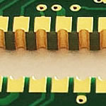
Semiconductor insulated heatsink conducting plate Aluminum mcpcb aplication
China PCB Manufacturing, Shenzhen PCB Manufacturer, Making Circuit boards
PCB Contract manufacturer, PCB Fabrication, Turnkey assembly services
Buy Print circuit board, customer: /USA/UK/Canada/South Africa...
PCB Supplier Shenzhen, China, PCB Manufacturer, Turnkey services
-
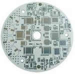
PCBSINO is the Top 5 PCB manufacturer company in China.
PCBSINO do rapid Prototype within 24 hours. our rigid PCB like MCPCB and Rogers PCB, FR4, High TG FR4, Rogers 4003, 4350,Al Aluminum metal Core MCPCB, Al2O3 Ceramic,Taconic,Halogen Free material, CEM-3, Fr2, CEM-1, CEM-2, 94VO, Rogers HF material, Polymide, etc.
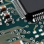
PCBSINO making many type electronic product for our customer, Our turkey services team can source original components part for your project(Digikey/Mouser/RS...), senior Electronic engineer will follow each step of the production to solve any PCB problem and our team will do final function test in PCB house.
Express PCB |
|
Rigid PCB Rapid Prototype,24 hours |
| Fr4 PCB |
|
prototype Lower to 15USD ! |
| Rapid Prototype |
|
Fr4 Rigid PCB Rapid Prototype China, |
MCPCB |
|
MCPCB Manufacturer China, Shenzhen |
| Aluminum PCB: |
|
Aluminum Metal Core PCB manufacturing, Fabrication |
| Aluminum PCB: |
|
single side, double side MCPCB, 0.5-5mm or more |
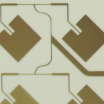
Rogers 4350B |
|
Rogers 4350,Rogers 4003 Manufacturing |
| Rogers 4350B |
|
Rogers 4350B,4003C PCB Manufacturer |
| Ro4350B |
|
Rogers High Frequency PCB Manufaturing China |
Turnkey Services |
|
Turnkey PCB Assembly Services, |
| Turnkey services |
|
Print circuit board Manufacturing, Turnkey Services |
| Turnkey Assembly |
|
Through Hole PCB components wave soldering Assembly |
Semiconductor insulated heatsink conducting plate Aluminum mcpcb aplication
-
Semiconductor insulated heatsink conducting plate Aluminum mcpcb aplication
Single Layer Metal Core PCB
A simple layer single sided MCPCB consists of a metal base (usually aluminum, or copper alloy), Dielectric (non-conducting) Layer, Copper Circuit Layer, IC components and solder mask.
The prepreg dielectric provides excellent heat transfer from the foil and components to the base plate, while maintaining excellent electrical isolation. The base aluminum/copper plate gives the single-sided substrate mechanical integrity, and distributes and transfers the heat to a heat sink, mounting surface or directly to the ambient air.
The Single-Layer MCPCB can be used with surface mount and chip & wire components, and provides much lower thermal resistance than FR4 PWB. The metal core provides lower cost than ceramic substrates, and allows much larger areas than ceramic substrates.
Double Layers Metal Core PCB
Double layers MCPCB is consisting of two layers of copper conductor, put them on same side of metal core (usually aluminum, copper or iron alloy). The metal base is on the bottom of whole MCPCB, which is different from double sided MCPCB(the two copper layers were put on the each side of metal core respectively), and you can only populate SMD on top side.
Different with Single layer MCPCB, 2 layers MCPCB requires an additional pressing step to laminate the imaged thermal conductive laminate and metal core (also known as metal base) together.
Compared with normal FR4, this sturcture need more technology and experience on laminating of two layers together with metal core.
The processing steps of the MCPCB with the metal base embedded in the PCB are comparatively complex as hole plugging is required after primary drilling on the metal base in order to isolate it from the circuitry.
Double Sided Metal Core PCB
It also has same two layers of copper conductor like Double layers MCPCB, but the metal core is in the middle of two conductor, so there're conductors (trace) on both sides of metal core, and were connected to each other by Vias. So we named it "Double sided MCPCB", and you can populated SMD on both top and bottom.
Different with Single layer MCPCB, double sided MCPCB also requires an additional pressing step to laminate the imaged thermal conductive laminate and metal core (also known as metal base) together. But sometimes, some raw Metal Clad material vendor will supply board material which already laminated.
Compared with normal FR4, this sturcture need more technology and experience on laminating of two layers together with metal core.
Multi Layers Metal Core PCB
Just like FR4 PCB, we can also make boards with more than 2 layers of traces and we named it "Multi Layers MCPCB". The structure is similar with FR4 Multi Layers, but it much more complex to make.
You can populated more components on the boards, put signal and ground layer into seperated layers, to achieve better performance in electrical performance.
Compared with normal FR4, this sturcture need more technology and experience on laminating of more than two layers together with metal core and the cost is much higher than 2 layers MCPCBor double sided MCPCB.
Heat dissipation has been a challenging issue in improving the reliability and life-time of electric devices. In particular, as high- power light emitting diodes (LEDs) generate substantial heat, heat dissipation must be considered when designing a LED module to secure the optical performance, photoelectric ef fi ciency and reliability [1 – 3]. Unlike in other electrical components, such as central procession unit and memory, a heat sink cannot be arranged on top face of the LED packages, because of the light emitting direction. Therefore, to reduce the rising temperature of the LED chip, the heat must be transmitted to the other side of the PCB, and thus to reduce the thermal resistance of LED module various studies have been conducted [4 – 8]. Among the studies to improve the heat dissipation, the metal-core printed circuit boards (MCPCBs), of which the substrate is made of metallic materials, is considered one of the most effective methods for reducing the junction temperature of LEDs [9,10]. Aluminum alloys are the most ideal substrate material because they have not only a high thermal conductivity but also a low density. If aluminum alloys are applied as the substrate material, most of the thermal resistance is taken by the insulation layer between the aluminum alloy substrate and copper circuit, because of the high thermal conductivity of the copper circuit and aluminum alloy substrate. Basically, a high breakdown voltage is required for the insulation layer. Accordingly, enhancing the thermal conductivity of the insulation layer, while maintaining the breakdown voltage, is a desirable research objective. In an attempt to reduce the thermal resistance of the insulation layer, an Al 2 O 3 and AlN aerosol deposition technique was adopted, and improved heat dissipation was reported [11,12]. However, the aerosol deposition is not suitable for the mass production and large size aluminum alloy substrate. If the aluminum alloys are used as a substrate of MCPCBs, the aluminum anodic oxide (AAO) layer, which is formed by electrochemical methods, can be applied to build up the insulation layer. Unlike the aerosol deposition, the anodic oxidation is advantageous for the mass production, manufacture cost and large size substrate. In addition, AAO is known to have a high insulating ability and have been reported to be suitable for the fabrication of hybrid integrated circuits [13 – 15]. For these reasons, some application methods of AAO for electric devices have been proposed [16,17]. In the present work, anodic oxidation known to a peculiar surface treatment of aluminum alloys was applied to form an insulation layer of a MCPCB. Electroless- and electro-deposition were used to form a copper circuit layer on the insulation layer. The heat dissipation performance of MCPCB with AAO layer was evaluated after mounting the LED package on the copper circuit layer. In addition, breakdown voltages of MCPCB with respect to the thickness of the AAO layer were measured. Al 1050 alloy (Al – 0.24Fe – 0.15Si, in wt.%) plate was used as the substrate for metal-core PCB. The specimen was cut into 30 mm  30 mm  2 mm sized pieces. Before anodic oxidation, the speci- mens were polished mechanically with 1500 grit SiC paper. Subsequently, etching in NaOH solution and activation in nitric acid were conducted. Before anodic oxidation, electro-polishing was conducted in perchloric acid/ethanol (1:4 vol.) electrolyte under a constant voltage of 20 V at 15 C for 2 min. Anodic oxidation was carried out in a 0.3 M oxalic acid electrolyte under a constant current density of 50 mA/cm 2 , and the electrolyte temperature was maintained at 10 C. The electrolyte and temperature condition were adopted from our previous research on the thermal conductivity of the AAO layer [18]. The thickness of the anodic oxide was controlled by the anodizing time. After anodic oxidation, the porous AAO was sealed in distilled water at 95 C for 30 min. AAO was etched in a 1.5 M NaOH solution for 30 s at room temperature to improve the adhesion of the epoxy layer. A thin polymer layer was build up on the AAO layer using a spray gun with a phenol-novolac type epoxy resin. This coated layer was cured in an oven at 130 C for 6 h. To improve the adhesion of the copper layer, a swelling treatment was conducted in a 25% 2-(2- butoxyetoxy)ethanol aqueous solution for 1 min at 80 C, followed by an oxidizing treatment by immersing the specimen in a 0.35 M KMnO 4 + 1.2 M NaOH solution for 1 min at 80 C. Separated SnCl 2 and PdCl 2 electrolytes as catalyzing procedures were used. Surface sensitization was achieved by immersing the oxidized specimen in a 0.08 M SnCl 2 + 0.29 M HCl solution at 25 C for 10 min. Catalyzation was then conducted in a 1.4 mM PdCl 2 + 29 mM HCl solution at 25 C for 10 min. A thin copper layer was deposited in an electrolyte containing CuSO 4 0.07 M, C 4 O 6 H 4 KNa 0.2 M, NaOH 0.3 M and HCHO 0.2 M at 25 C for 10 min. A thick copper layer was then grown by electro-deposition in a pyrophos- phate copper electrolyte. Surface morphologies and cross section of the prepared MCPCB were observed using fi eld emission electron scanning microscopy (FE-SEM). The thermal resistance and breakdown voltage of MCPCB were measured using a thermal transient tester (T3Ster) and a withstanding voltage tester (TOS5101), respectively. The breakdown voltages were determined by sweeping the applied voltage to copper circuit layer and aluminum alloy substrate until the current reaches 0.1 mA. In order to improve the accuracy of obtained breakdown voltage, fi ve samples with a same AAO thickness were measured and averaged. To measure the thermal resistance using T3Ster, a LED chip (CREE XP-G LED Cool White R4) was mounted on the prepared MCPCB using a silver paste solder. Three samples with a same AAO thickness were prepared for the measurements using T3ster, and the measurement was repeated three times for each sample. Surfaces and pore morphology of AAO were observed after sealing and etching, and images are shown in Fig. 1. AAO is composed of a hexagonal columnar cell with a high aspect ratio cylindrical pore at the center. Therefore, exposed circular pores could be observed on the AAO surface (Fig. 1(a)). The thermal conductivity of AAO grown under the abovementioned conditions was reported to be 1.62 W m À 1 K À 1 [18]. A dense oxide layer without pores is desirable for the thermal conductivity of AAO, but cylindrical pores are inevitable during the growth. Therefore, to improve the thermal conductivity of the AAO, hydrothermal sealing was used to plug the nano-sized pores. To achieve a completely sealed AAO, the residual water in pores, which was reported to be helpful to seal the inner pores, was allowed to remain before sealing [19]. The morphology of inner pores is shown in Fig. 1(b) and all of the pores were fi lled with boehmite (AlO Á OH), which is known as a sealant of hydrothermal sealing [20,21]. It was reported that stress between the AAO and aluminum alloy substrate were generated during the hydrothermal sealing and sometimes that results in surface cracks [22,23]. In addition, precipitates, intermetallic compound, and inclusions, involved in the aluminum alloy substrate are known to cause some irregular surface of the AAO [24 – 26]. During the electroless copper deposition processes, Sn 2+ , Pd 2+ and Cu 2+ ions can be absorbed in cracks and irregular surface, and then they migrated toward the aluminum alloy substrate. Absorbed elements have higher reduction potential than aluminum, thus tin, palladium and copper precipitation on the substrate are possible by the replacement reaction. Sometimes precipitated particles on the substrate electrically contact with the copper circuit layer formed by electroless deposition, thus the anodic oxide layer cannot secure the electrical insulation between aluminum alloy substrate and copper circuit layer [27]. In the present work, to perfectly avoid the absorption of metallic ions, a thin epoxy layer was coated on the AAO. A phenol- novalac type epoxy resin, used in this study, is well-known to have high electrical insulation and thermostability [28,29]. Therefore, a number of studies on the electroless deposition on the phenol- novalac type epoxy, which have been usually applied to electric devices have been carried out [30 – 32]. To enhance the adhesion between the epoxy and anodic oxide layers, an etching of anodic oxide was conducted in NaOH solution before the epoxy coating and a roughened surface can be observed as shown in Fig. 1(c). Surface morphologies after epoxy coating, roughening and copper deposition are shown in Fig. 2. Since the adhesion between the epoxy and copper layers is mainly dependent on the mechanical interlocking, poor adhesion was expected because of the smooth surface of the epoxy coating layer (in Fig. 2(a)). Therefore, to enhance the adhesion the surface roughening was carried out.
Shifting light production from filaments, gas discharges and arcs to semiconductors brings about many changes to the lighting field, which has not changed basic technology much in the last 50 years. As seen again in Table 1, conventional lighting sources reject most of the waste energy as infrared heat radiation, and this has led to fixtures and systems optimized for this mode of heat transfer (with convection also applicable to fluorescents). If the reader places his hand in front of one of these sources, there is a considerable feeling of heat on the skin.
However, heat transfer for semiconductors is first a conduction problem, and with LED junction temperatures limited to less than approximately 100°C (in most cases), conduction is the primary transfer method until a suitable area for natural convection is reached. Radiation is small between the die and the system because the LED source is cooler than a filament or an arc. This differentiates LEDs from other lighting sources where most heat is radiated to the environment from non-LED light sources.
Instead of most of the thermal energy leaving the source by radiation, an LED system’s thermal energy leaves via the fixture at a much lower temperature with a mix of primarily natural convection and some radiation. This change in the cooling mechanism for lighting systems cannot be understated, as system designers are not used to thinking and designing for this different thermal system. A suitable path for conducting heat from the LEDs must be provided, and that also includes the various thermal interfaces in the system (often which are just simple sheet metal fixtures with poor contact between parts).
Figure 1. LED package changes.
Moving the Heat
LED packages have changed through the last decade to adapt to higher conductive power dissipations. Originally, the 5 mm and 3 mm packages were used as indicators, and these were pressed into service for new die luminaries. However, with 300°C/W for thermal resistances, these packages were not suitable for the increasing powers necessary to meet the light level demand. Figure 1 shows the changes in LED packages during the last decade, with chip on board (COB) devices having the best performance at about 5-10°C/W to the circuit board substrate. Leadframe modifications dominated the early changes until power requirements necessitated the use of a central heat-conducting slug in packages. Figure 2 shows a typical power package design with a central heat slug.
Figure 2. Power Package LED Cross Section (courtesy Lumileds).These modifications to the LED packages motivated changes to the circuit boards to handle the increased heat dissipation. With large powers dissipated from the LED leads, and now the central thermal slugs, boards have quickly changed to move this heat appropriately. It is possible to still use standard FR-4 technology boards for LEDs up to 0.5 W dissipation, but above that some metallic substrates are required.
Hall-Effect Sensors
A Hall-effect sensor is a transducer that varies its output in response to slight changes in magnetic fields. Commonly used for proximity switching, positioning, pressure, speed detection, fluid flow, and current sensing.
Hall-Effect Switches
Hall-effect switches generally incorporate an IC chip containing a Hall generator, trigger circuit, and amplifier. Depressing the switch moves a magnetic shunt member and, via the Hall effect, switches the trigger circuit to its on state.
Hall Probes
A semiconductor-based detector which uses the Hall effect to measure the strength of a magnetic field. Probe contains an indium-compound crystal mounted on an aluminum-backing plate and encapsulated in the probe head.
Hand-Held Enclosures
Small enclosures that can accommodate a variety of electronic assemblies. Most are molded cases consisting of a top, base, and cover, having an ergonomic profile for comfortable holding.
Hardmetric Connectors
Hardmetric connectors use a dense pin grid of 2.00 mm and meet requirements of the IEC 61076-4-101 standard. Connectors suitable for use in high-speed data, telephony, CompactPCI applications, and feature high-density and fast-signal transmission.
Hardware Component Accessories
Handles, drawers, slides, etc. are all hardware components which are accessories to enclosures, cabinets, racks, etc. assemblies. These peripheral items ease the operator’s interface and usability of the equipment.
Harmonic Filters
A combination of inductance and capacitance tuned to an undesired harmonic to suppress its amplitude and protect electrical equipment from damage due to harmonic-voltage distortion.
HD
High density or high definition. Can refer to a high-capacity optical storage medium, such as a high-capacity DVD. As a measure of pixel density (resolution) it can refer to computer displays, image scanners and digital camera image sensors.
Ceramic Heat Dissipation—Less Is More - Electronic Design The ceramic heat sink CeramCool is an effective combination of circuit board and heat sink for the reliable cooling of thermally sensitive components and circuits.
Is a composite granite sink better than a stainless steel sink? - Quora What does a heat sink look like? When do you change your kitchen sink? How do you remove a drain from a sink? Why are sinks flat? How do I sink a Fitbit?
Efficiency and Cost Tradeoffs Between Aluminum and Zinc- Aluminum Die Cast Heatsinks Efficiency and Cost Tradeoffs Between Aluminum and Zinc-Aluminum Die Cast Heatsinks Kurtis P. Keller University of North Carolina, Computer Science Department
Patent US20120307501 - Led plastic heat sink and method for making and using the same - Google Patents and an aluminum heat sink 16, with screws 10 enabling the tight assembly between the printed circuit board package 12 and the aluminum heat sink
Benchtest.Com - Aluminum and Copper Heat Sink After my last few projects, I had come to understand a bit more on basic heat sink design and decided that it was time to move to what I considered the next step. Up to this point, all of my heat sinks had been made of aluminum. I had done some playing with copper
Patent US6069023 - Attaching heat sinks directly to flip chips and ceramic chip carriers - Google Patents An aluminum or copper heat sink is attached to a ceramic cap or exposed semiconductor chip using an adhesive of silicon or which results in a CTE difference of 18.9 ppm/ C. The ceramic top is a relatively smooth surface and any delamination or cracking
Metal Core PCB | MCPCB | Aluminum PCB | Copper Core PCB | LED PCB - Best Technology As Metal Core PCB means the base material for PCB is metal, and currently the most common metal used are Aluminum, Copper alloy. Majority of MCPCB are made of aluminum for LED Lamps. Metal Core Printed Circuit Board Home Products Metal Core PCB
Headphones, Handsets & Chestsets
Headphones refer to a pair of tiny speakers worn over the ears. When phones are connected to a source this allows user to listen to audio. A headset is a microphone/headphone used in telecommunications. Chestsets used with headsets and allow portability.
Today it is common to find a metal core printed circuit board (MCPCB), also known as an insulated metal substrate (IMS) board, in use underneath 1W and larger devices. These typically have a 1.6 mm (1/16″) base of aluminum with a dielectric layer attached, followed by copper trace layers and solder masks. The aluminum sheet metal allows the heat to move efficiently away from the LED to the system. Other developments with graphite or copper layers in FR-4 PCBs are under development and may provide alternatives to standard MCPCBs. For extremely high performance applications, ceramic-based systems are available for circuitry.
Application of MCPCB
LED lights:High-current LED, Spotlight, high-current PCB
Industrial power equipment:High-power transistors, transistor arrays, push-pull or totem pole output circuit (to tem pole), solid-state relay, pulse motor driver, the engine Computing amplifiers (Operational amplifier for serro-motor), pole-changing device (Inverter)
Cars:firing implement, power regulator, exchange converters, power controllers, variable optical system
Power:voltage regulator series, switching regulator, DC-DC converters
OA:Printer driver, large electronic display substrate, thermal print head
Audio:input - output amplifier, balanced amplifier, pre-shield amplifier, audio amplifier, power amplifier
Others:Semiconductor thermal insulation board, IC arrays, resistor arrays, Ics carrier chip, heat sink, solar cell substrates, semiconductor refrigeration device
For furhter information, please feel free to contact us, www.pcbsino.com