Gerbview Gerber tools
China PCB Manufacturing, Shenzhen PCB Manufacturer, Making Circuit boards
PCB Contract manufacturer, PCB Fabrication, Turnkey assembly services
Buy Print circuit board, customer: /USA/UK/Canada/South Africa...
Gerbview Gerber tools
-
CAD / CAM Software Solutions
Downloads
GerbView 7
http://www.gerbview.com/download.html
Gerber Viewer and Converter
HOME
PURCHASE
SUPPORT
DOWNLOAD
OTHER PRODUCTS
RESELLERS
COMPANY
GerbView
Gerber Viewer and Converter
View, print and convert Gerber, ODB++, PDF and Excellon
Convert to PDF, DXF, DWF, RS-274X, TIFF, SVG and more
GerbView™ can view, print and convert Gerber, Extended Gerber, ODB++, PDF, Excellon, PLT, HPGL/2 and other file formats.
GerbView
GerbView™ is an advanced but easy to use application that enables you to view, print and convert Gerber, ODB++, Adobe PDF, Excellon and HPGL/2 files.
GerbView supports RS-274D and RS-274X Gerber formats, and you can use it to convert your older Gerber files to the new RS-274X extended format. The new extended Gerber format contains embedded aperture information, and using this format will minimize the risk for errors during the manufacturing of the PCB.
With GerbView's PDF to CAD capability you can convert your Adobe PDF files to Gerber or Autodesk DXF.
Gerbview will visualize your design, on the screen or in hardcopy. No more waiting for photoplots or your prototype circuit board, to see your true design.
You can use the measure and query tools to check apertures, tools, pens, distances and areas.
In GerbView you work with a workspace that can contain one or more files of the supported file formats. The workspace can be saved for later use. The saved workspace will link to your design files, so only need to reload the workspace file to see the whole design.
Markup elements like text, barcodes, arrows, lines, images, ellipses and polygons can be added to the workspace. Markups will be stored in a separate file.
GerbView can convert your Gerber, HPGL/2 and Excellon files to Autodesk DXF, Autoesk DWF, Adobe PDF and other formats. You can combine several different Gerber files (layers) and create a multi-layered PDF, DXF or DWF file. See list of supported formats below.
GerbView can rasterize single files, or whole workspaces, and save to one of the supported raster formats. Markup elements can optionally be included in the conversion.
You may print scaled or in real size. All Windows based plotters and printers are supported. Poster mode, also known as tiled pages, can be used to print large designs and drawings on for example several smaller A4/Letter pages.
Gerbview
DescriptionFeatures & FormatsUpdatesScreenshotsPrices
Gerbview will visualize your design, on the screen or in hardcopy. No more waiting for photo plots or a prototype circuit board, to see your true design.
GerbView supports both RS-274D and RS-274X Gerber formats, and you can use it to convert your older Gerber files to the new RS-274X extended format. The newer extended Gerber format contains embedded aperture information, and this minimizes the risk for errors during the manufacturing of the PCB.
With GerbView's PDF to CAD capability you can convert your Adobe PDF files back to editable Gerber RS-274X and DXF files.
GerbView can create layered PDF, DXF and DWF files where each loaded Gerber file will correspond to a separate layer in the destination file. Check out our blog and read more about how you can create layered PDF files with GerbView. You may in addition create a multi-page PDF file from all loaded layers, where each layer will be placed on its own page in the output file.
With GerbView you can export individual layers, or the whole workspace, to any of the supported raster formats, which includes TIFF, JPEG, PNG and BMP. The resolution and number of colors used for the conversion can be set by the user.
Convert PDF to Gerber, SVG, HPGL/2 and DXF
Convert PDF to Gerber,
SVG, HPGL/2 and DXF
In GerbView you work with a workspace that can contain one or more files (layers) of any of the supported file formats. The workspace can be saved for later use. The workspace will reference your design files, so only need to reload the workspace to see the whole design. You can set the size of this workspace to one of the preselected paper sizes, or to a custom size.
Use the precise measure tool to verify distances and areas. Check apertures used by tracks and flashes using the query and aperture highlight tools.
Markup elements like text, barcodes, QR-codes, images, arrows, lines, symbols, ellipses and polygons can be added to the workspace, and will be included during conversion and printing.
All types of markup elements, for example text or barcode, may be "burned-in" to become a permanent part of a Gerber layer.
You may print your files using a custom scale, for example 100% for original scale, or using fit to page. The print poster mode, also called tiled pages, can be used to print large designs and drawings on multiple sheets. Header, footer and watermark information can optionally be added to the printed sheets.
Try GerbView Now
Feedback
Please direct any bug reports, suggestions or new versions to here:
About KiCad document: https://github.com/KiCad/kicad-doc/issues
About KiCad software: https://bugs.launchpad.net/kicad
About KiCad software i18n: https://github.com/KiCad/kicad-i18n/issues
Publication date and software version
Published on February 14, 2015.
1. Introduction to GerbView
GerbView is a Gerber file viewer (RS 274 X format), and is also able to display drill files from Pcbnew (in Excellon format).
It accepts up to 32 files (Gerber and/or Drill files)
Files can be displayed using a transparency mode or stacked mode.
For more information about the Gerber file format please have a read at the specification in The Gerber File Format Specification - Ucamco.
2. Main Screen
gerbview_main_screen_png
3. Top toolbar
gerbview_top_toolbar_png
gerbview_clear_layers_png
Clear all layers
gerber_file_png
Load Gerber files
gerbview_drill_file_png
Load drill files (Excellon format from Pcbnew)
sheetset_png
Set page size for printing and show/hide page limits
print_button_png
Open print dialog
zoom_in_png zoom_out_png
Zoom in and out
zoom_redraw_png
Refresh screen
zoom_fit_in_page_png
Zoom fit in page
gerbview_top_layer_png
Layer selection
gerbview_top_dcode_png
D Code selection (hight light items that use this dcode)
gerbview_top_info_png
Info about Gerber file options loaded in the current layer
4. Left toolbar
Gerbview
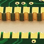
Loading in finished Gerbers for checking is a last step in designing a PCB.
Related kicad pages
EE CAD Terminology
kicad Navigator - the kicad project Manager
eeschema - the schematic editor
cvpcb - the component to module (AKA foot-print) editor
pcbnew - the PCB layout program
Gerbview - the Gerber file viewer and production notes
Bitmap2Component Converts bitmap images to filled polygons
wings3d - 3d view - good way to waste a lot of time..
Similar Gerber viewer
In Debian install gerbv - it has differnet features - some better some worse than gerbview
Checklist
Super Money saving tip: print out the artwork on card-stock 1:1 and poke holes and stuff it like a real PCB - find errors - fix them and rework for pennies all the same day..
Part Placement
SMD component orientation consistent
Clearance for IC extraction tools, heatsinks etc.
Polarization of components checked
Are components on grid ?
Check the orientation of all connectors - is Pin #1 where you expect it?
minimum component body spacing
Bypass capacitors located close to IC power pins
Series terminators are located near the source
I/O drivers near where their signals leave the board
PCB has ground turrets, power rail test points, and test points for important signals, all labeled
EMI and RFI filtering as close as possible to exit and entry points in shielded areas
Potentiometers should increase controlled quantity clockwise
Mounting holes electrically isolated or not?
Mounting hole clearance for hardware
SMD pad shapes checked
Tooling holes for automated assembly
Extra clearance for socketed ICs
Pin one pad indicators
Routing
Digital and analog signal commons joined at only one point - net tie - ground Pavilion
Check for traces running under noisy or sensitive components
No vias under metal-film resistors and similar poorly insulated parts
Traces spaced to max where possible
Check for dead-end traces, unless used on purpose
Ensure schematic software did / did not separate Vcc from Vdd, Vss from GND as needed (Not a problem if you don't use invisible
connections - it really doesn't save time in the long run )
Multiple vias for high current and/or low impedance traces - check the current ratings of your via size
Current rating of Traces, viass
Wire-Gauge_Ampacity
Tips for PCB Vias Design Engineering articles from Quick-teck PCB manufacturer
IPC trace width chart
Via calculations
current vs Trace temperature rise
Trace fusing currents
Component and trace keepout areas observed
Ground planes where possible
Dimensions
Hole diameter on drawing are finished sizes, after plating.
Finished hole sizes are >= 0.25mm larger than lead
Silkscreen legend text weight, spacing
Pads >=0.37mm larger than finished hole sizes
Components spacing from edge of PCB
Traces to board edge spacing
Consider Drill size tolerance
Soldermask clearance and tolerance - often board houses want zero clearance.
High voltage traces need extra spacing
Text on Silk Screen and other Layers
Allign legend text tp read from one or two orientations
Logo in silkscreen legend
Copyright notice
PCB part number and version
Do parts cover Legend
Label all layers - Mirror text on back
Pin one indicators
High pin count parts can have corner pins numbered for ease of location
Silk screen tick marks for every 5th or 10th pin on high pin count Parts
Other
CAD design rule checking must be turned on
High frequency circuitry precautions observed
ReadMe for PCB house see Gerbview#What_to_send_the_PCB_house checklist
Thermal reliefs for internal power layers
Solder paste mask spacing
Blind and buried vias on multilayer PCB
PCB layout panelization
Standard Sizes
Drill sizes: Drill_Bit_Conversion_Table
Gerber file names
x.gba Bottom Adhesive
x.gbl Bottom copper
x.gbo Bottom Silk-screen
x.gbp Bottom Solder-Paste
x.gbr board outline - edges
x.gbs Bottom Solder-mask
x.gko keep out ( Not yet implemented 2013-07 )
x.gta Top Adhesive
x.gtl Top copper
x.gto Top Silk-screen
x.gtp Top Solder-Paste
x.gts Top Solder-mask
Inner Layers
x.gp1 - inner plane 1 - Negative
x.gp2 - inner plane 2 - Negative
x.g1 - inner routing layer 1
x.g2 - inner routing layer 2
What to send the PCB house
All the gerbers and a README.txt are packed up into a tar. ark is a great tool for this.
The README.txt should look something like this:
Contact name
phone
email
address
>>>- hole dimensions are finished size- <<<<<
-PCB Name and revision number: DC_UPS3.1
Use this name on invoices
-We provide Gerber files including drill layer
Pads 23 Through vias 16 Smallest hole .025" (0.64mm) Specified finished size. 39 holes
-FR406 or 370HR 1.57mm[.062"] IPC-4101C Sheet 24
-Copper thickness 0.0347mm [1oz]
-Quantity 4
-Sides 2
-HASL
-Silk Screen 2 sides (white or yellow)
-Solder Mask 2 sides green/matte finish SR1000 over bare copper (same art work) to IPC-7351
-Size 50 x 65mm
-To IPC specifications
- For productions quantities please Quote -
Solder resist (solder mask) is required on both external faces of the printed board, it shall meet
the qualification/conformance IPC-SM-840. Coverage, cure and adhesion shall be as defined in
paragraphs 3.8.1 to 3.8.3 of IPC-6012, except that no encroachment of solder resist is allowed on
any surface mount or ball grid lands, and that ALL pad patterns have solder resist slivers between
individual pads. The height of the solder resist should not cause any mounting problems for
surface-mount components.
gerbview_left_toolbar_png
grid_png
Grid on / off
polar_coord_png
Display polar coordinates on / off
unit_inch_png unit_mm_png
Units selection to display coordinates
cursor_shape_png
On grid cursor shape selection
pad_sketch_png
Display mode selection (solid or outlines) for flashed items
track_sketch_png
Display mode selection (solid or outlines) for lines
opt_show_polygon_png
Display mode selection (solid or outlines) for polygons
gerbview_show_negative_objects_png
Show negative objects in ghost color
show_dcodenumber_png
Show / hide D Codes values (for items using a dcode)
gbr_select_mode0_png gbr_select_mode1_png gbr_select_mode2_png
Mode used by Gerbview to show layers.
5. Commands in menu bar
Gerbview: remove analysis of fully outdated (and never used) gerber c… …
..
dialogs Refactor layer enumerations to all live in the same place 5 months ago
gerber_test_files Gerbview: fix a subtle issue when reading parameter values in Gerber … 5 months ago
CMakeLists.txt Multiple improvements concerning colors, configuration handling and l… 17 days ago
Info.plist Changed the bundle identifier to org.kicad-pcb. to follow the ki… 2 years ago
block.cpp Change from EDA_COLOR_T to COLOR4D globally; arbitrary color support 6 months ago
class_DCodeSelectionbox.cpp Gerbview: better management of d_codes list in toolbars. a year ago
class_DCodeSelectionbox.h Gerbview: better management of d_codes list in toolbars. a year ago
class_X2_gerber_attributes.cpp Pcbnew: Add creation of Drill Files in Gerber X2 format. 4 months ago
class_X2_gerber_attributes.h Pcbnew: Add creation of Drill Files in Gerber X2 format. 4 months ago
class_am_param.cpp Fix Coverity warnings 3 months ago
class_am_param.h Gerbview: evaluate Aperture Macro Parameters using precedence rules f… 4 months ago
class_aperture_macro.cpp Gerbview: fix an issue (crash or hang) when a aperture macro definiti… 4 months ago
class_aperture_macro.h Gerbview: fix an issue (crash or hang) when a aperture macro definiti… 4 months ago
class_excellon.h Add more "override" markers. 11 months ago
class_gbr_display_options.h Changed COLOR4D defines to static consts 6 months ago
class_gbr_layer_box_selector.cpp Multiple improvements concerning colors, configuration handling and l… 17 days ago
class_gbr_layer_box_selector.h Change from EDA_COLOR_T to COLOR4D globally; arbitrary color support 6 months ago
class_gbr_layout.cpp Change from EDA_COLOR_T to COLOR4D globally; arbitrary color support 6 months ago
class_gbr_layout.h Fix a few doxygen warnings 2 months ago
class_gbr_screen.cpp Code cleanup: Remove outdated decimils to/from iu defines and convers… a year ago
class_gbr_screen.h Explicitly mark overriding functions. 11 months ago
class_gerber_draw_item.cpp Drill dialog: creates the directory, when the path entered in dialog … 4 months ago
class_gerber_draw_item.h Change from EDA_COLOR_T to COLOR4D globally; arbitrary color support 6 months ago
class_gerber_file_image.cpp Gerbview: remove analysis of fully outdated (and never used) gerber c… 10 days ago
class_gerber_file_image.h Gerbview: remove analysis of fully outdated (and never used) gerber c… 10 days ago
class_gerber_file_image_list.cpp Pcbnew: Add creation of Drill Files in Gerber X2 format. 4 months ago
class_gerber_file_image_list.h Gerbview: fix a crash when reading polygons with arcs. a year ago
class_gerbview_layer_widget.cpp Refactor layer enumerations to all live in the same place 5 months ago
5.1. File menu
gerbview_file_menu_png
It is possible to load gerber and drill files into Gerbview. There is also an auxiliary option to export gerbers to pcbnew. Previously (a long time ago) it was also possible to load so called Dcodes, but those are now obsolete and is therefore not possible anymore.
5.1.1. Export to Pcbnew
GerbView has a limited capability to export Gerber files to Pcbnew.
The final result depends on what features of RS 274 X format are used in Gerber Files.
RS 274 X format has raster oriented features that cannot be converted (mainly all features relative to negative objects).
Flashed items are converted to vias.
Lines items are converted to track segments (or graphic lines for non copper layers)
So the usability of the converted file is very dependent upon the way each Gerber file was built by the original Pcb tool.
PCB Supplier Shenzhen, China, PCB Manufacturer, Turnkey services
-
PCBSINO is the Top 5 PCB manufacturer company in China.
PCBSINO do rapid Prototype within 24 hours. we can make Flexible Print circuit boards and Rigid circuit boards, like FR4, High TG FR4, Rogers 4003, 4350,Al Aluminum metal Core MCPCB, Al2O3 Ceramic,Taconic,Halogen Free material, CEM-3, Fr2, CEM-1, CEM-2, 94VO, Rogers HF material, Polymide,Flexible PCB FPC etc.
we already made many type electronic product for our customer, Our turkey services team can source original components part for your project, senior Electronic engineer will follow each step of the production and do function test in PCB house.
Express PCB |
|
Rigid PCB Rapid Prototype,24 hours |
| Fr4 PCB |
|
prototype Lower to 15USD ! |
| Rapid Prototype |
|
Fr4 Rigid PCB Rapid Prototype China, |
Turnkey Services |
|
Turnkey PCB Assembly Services, |
| Turnkey services |
|
Print circuit board Manufacturing, Turnkey Services |
| Turnkey Assembly |
|
Through Hole PCB components wave soldering Assembly |
For furhter information, please feel free to contact us, www.pcbsino.com