orcad_10.3 PCB design tools
China PCB Manufacturing, Shenzhen PCB Manufacturer, Making Circuit boards
PCB Contract manufacturer, PCB Fabrication, Turnkey assembly services
Buy Print circuit board, customer: /USA/UK/Canada/South Africa...
PCB Supplier Shenzhen, China, PCB Manufacturer, Turnkey services
-
PCBSINO is the Top 5 PCB manufacturer company in China.
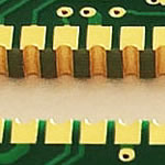
PCBSINO do rapid Prototype within 24 hours. we can make Flexible Print circuit boards and Rigid circuit boards, like FR4, High TG FR4, Rogers 4003, 4350,Al Aluminum metal Core MCPCB, Al2O3 Ceramic,Taconic,Halogen Free material, CEM-3, Fr2, CEM-1, CEM-2, 94VO, Rogers HF material, Polymide,Flexible PCB FPC etc.
we already made many type electronic product for our customer, Our turkey services team can source original components part for your project, senior Electronic engineer will follow each step of the production and do function test in PCB house.
Express PCB |
|
Rigid PCB Rapid Prototype,24 hours |
| Fr4 PCB |
|
prototype Lower to 15USD ! |
| Rapid Prototype |
|
Fr4 Rigid PCB Rapid Prototype China, |
Turnkey Services |
|
Turnkey PCB Assembly Services, |
| Turnkey services |
|
Print circuit board Manufacturing, Turnkey Services |
| Turnkey Assembly |
|
Through Hole PCB components wave soldering Assembly |
orcad_10.3 PCB design tools
-
orcad_10.3
pspice.exe, RunDll32.exe, allegro.exe, CAPTURE.EXE . OrCAD PCB design . APP is FREE for users on the most current releases of OrCAD Capture CIS .Allegro Sigrity Serial Link . Allegro Design Entry Capture/Capture CIS . I did export the netlist from Orcad capture and import in Orcad PCB editor and .Orcad 10.5 Crack Pspice PCB Editor Capture CIS 3 download . 795 MBTorrent ContentsOrcad 10.5 Crack Pspice PCB Editor Capture CIS Crack Orcad 10.5 by RiSEReadMe .Seeds:4 Leech:0 795.2 Mb Orcad 10 5 + Crack Pspice + PCB Editor + Capture CISSubmit a problem report for ni multisim. Orcad 10.5 crack pspice pcb editor capture cis by bananas teamNote: For the I/O Editor dialog to open, . Creating Schematic Symbols using Cadence OrCAD Capture CIS for SmartFusion2 and IGLOO2 Designs 20 Power .System Serial Link Option; Package . OrCAD PCB Design Flow OrCAD Capture i PCB Editor . Program moe by dodatkowo rozbudowany o moduy takie jak opcja CIS czy .Headquartered in San Diego, California, LifeProof is a consumer electronics accessory company acquired in 2013 by OtterBox.Low Prices on Pspice Orcad . Free 2-Day Shipping w/ Amazon Prime.Visit us and download orcad capture absolutely for free. Free downloads. . Orcad 10.5 + Crack (Pspice + PCB Editor + Capture CIS) >> music - other: 2 months ago .
engineering department offers Schematic Capture, PCB Layout and Library Creation services. All projects are done by experienced electronic engineer and expert user of DipTrace Schematic and PCB Design software. Our staff will work with you till the project is done without overcharging.
using orcad10 Layout plus and i want to design a footprint of 8 pin SOIC the problem is that i am not able to shrink the size of the pad in the top layer below a certain value and also i am not able to change the shape of the pad in the top layer. I am trying to design a PCB where in i am using both SOIC and PDIP package IC's
Pl let me know how to Design SOIC Footprint in Top Layer. I am using Library manager in Orcad Layout Plus.
Orcad Layout Plus Tutorial Layout Plus is a circuit board layout tool that accepts a layout-compatible circuit . (ex., from Capture CIS schematic) to the PCB.Orcad 10.5 + Crack (Pspice + PCB Editor + Capture CIS) : 795.20 MB . Orcad 10.5 + Crack (Pspice + PCB Editor + Capture CIS)by RiSE+.zip.How to install and crack Orcad 16.6 Full - Duration: . How to install OrCAD Capture v16.6 (PSpice) . How to install Orcad 16.6 and orcad 10.5 .. the Cadence OrCAD Capture Property Editor with the high . OrCAD lite is a great way to learn the OrCAD tools and . OrCAD PCB Designer or OrCAD PSpice .. this is the tool of choice for rapid design capture. * OrCAD PCB Editor, . crack. Cadence Orcad Suite With Pspice 10.5 . (Capture and PSpice only) CIS .Orcad 10.5(Pspice + PCB Editor + Capture CIS)/Crack/1143798839[1].pdf 269.02 KB; Orcad 10.5 . Orcad 10.5(Pspice + PCB Editor + Capture CIS)/Crack/orcadv105.dat 1 .
Based on production-proven Allegro PCB technology, OrCAD PCB Editor offers a wide array of powerful features to speed designs from placement and routing through to manufacturing.
OrCAD™ PCB Designer is a tiered, scalable PCB design solution that delivers advanced capabilities and highly integrated flows. The powerful, tightly integrated PCB design technologies include schematic capture, librarian tools, PCB editing and routing (PCB Editor), Constraint Manager, signal integrity (included in Professional), autorouting (included in Professional), and optional mixed-signal circuit simulation. The PCB Design Suites contain proven OrCAD and Cadence® Allegro® technology for a consistent design process. These tools have
OrCAD Standard
Concept to Production Design Environment
Integrated front to back design environment
OrCAD Capture schematic entry
Pre-layout SI analysis
PCB editing with OrCAD PCB Editor
Real-time DRC
Rigid-Flex design support
Constraint manager
3D ECAD MCAD co-design
DFM analysis and manufacturing outputs
Altium, Eagle, and PADS translators
Article Technical Rating: 7 out of 10
There are numerous software packages available for designing printed circuit boards (PCBs), too many in fact.
That being said, there are three PCB design packages that are the most popular: Altium, Eagle, and OrCad.
For a struggling hardware entrepreneur developing a new electronic product or even for a freelance engineer just getting started, all three of these packages are probably prohibitively expensive. Launching a new product is already rather expensive without also spending thousands of dollars on just design design software.
NOTE: Whether you're a maker, inventor, or engineer if you want to develop a new electronic hardware product then download your free cheat sheet - 15 Steps to Develop Your New Electronic Hardware Product.
Altium Designer is considered the Ferrari of PCB design packages and starts at over $7,000! No that is not a typo. It’s good software, but that’s pretty crazy.
Altium is the most popular PCB design package among those with a company’s budget behind them. Because of that it’s also the package that many new freelance engineers are most familiar. A good amount of freelancers splurge on Altium because it’s what they already know.
Most people developing PCBs independently, like entrepreneurs, hackers, and freelance designers, usually can’t afford to shell out that kind of cash on software.
when we went into more details, the Orcad PCB Designer Professional started looking to me more like a trap. Don’t forget, once you start using it, it’s very difficult to move to a different software. And if your company grows and you do more and more complex boards, you may very easily find the limits of Orcad Professional. That day, when I was leaving the Cadence stand, the conclusion was: I would need to pay at least 25000 EUR for the configuration which can be used for professional HW design + around 20% fees every year.
Top PCB Design Software Tools for Electronics Engineers: 46 Must-Have Tools to Streamline PCB Design
Last Updated: Feb 23, 2017 | by Trey Hooper | Engineering | 0 comments
No matter which project it is that they are working on, electronics engineers must know exactly how the electrical circuits should be laid out and how they will work. Without printed circuit boards (PCBs), an electronics engineer’s job would be impossible. But, it can be quite a task for an electronics engineer to find the right PCB design software tools because they are so busy and there are so many to sift through.
That’s why we have pulled together 46 of the top PCB design software tools for electronics engineers – to save you time while you are designing your projects. We also realize that one software tool may be appropriate for one PCB project while another will work better for other types of projects. As a result, we have included simple tools, free tools, and proprietary tools on our list. Our criteria was simple: the PCB design software tools for electronics engineers must be intuitive, include useful features, be established enough to limit risks, and feature a robust library so they can be applied to multiple projects. We share our top 46 PCB design software tools for electronics engineers here, in no particular order.
You can easily compare Orcad PCB Designer Standard / Professional and Allegro Designer by yourself in this document (or see the original here). As you can see, Orcad Standard doesn’t even include Differential pair routing (essential for any board), and Orcad Professional doesn’t have Propagation delay rules (essential for memory layout).
So, if you want to use the Orcad PCB Designer for all your future designs and you are sure you are not going to design any boards with differential pairs or memories – go for it. If you are planning to do layout professionally and you are planning to grow and design more and more complex boards, be sure you have considered all the option and made the right decision.
OrCAD PCB Editor
Based on production-proven Allegro PCB technology, OrCAD PCB Editor offers a wide array of powerful features to speed designs from placement and routing through to manufacturing.
Cadence® OrCAD® PCB Designer contains a fully integrated design flow that includes:
Constraint manager
Design capture technology
Component tools
PCB editor
Auto/interactive router
Interfaces for manufacturing and mechanical CAD
At the heart of OrCAD PCB Designer is OrCAD PCB Editor, an interactive environment for creating and editing simple to complex multi-layer PCBs. The extensive feature set addresses a wide range of design and manufacturability challenges. OrCAD PCB Designer and OrCAD PCB Designer with PSpice both include Cadence SPECCTRA® for OrCAD, the market-leading PCB solution for automatic and interactive interconnect routing. Designed to handle routing challenges requiring complex design rules, it uses powerful shape-based algorithms for speed and efficient use of the routing area. Optional PSpice® circuit analysis and simulation capabilities integrated with the included OrCAD Capture facilitates rapid design-and-simulate cycles, allowing engineers to explore various design configurations before committing to a specific circuit implementation.
A common database architecture, use model, and library offer truly scalable PCB solutions for both OrCAD and Allegro products, allowing engineers the ability to migrate to the Allegro PCB technologies as their designs and design challenges increase in complexity.
Outstanding Technology
OrCAD technologies provide maximum robustness and functionality depth to meet the most demanding customer requirements for all types of designs
Fully Customizable
The OrCAD open architecture platform allows you to add new functionality in the form of apps, or you can build capability and flows yourself.
Complete Design Solution
OrCAD® PCB solutions provide a complete environment from initial schematic to final artwork. The platform delivers a complete, integrated workflow.
engineering department offers Schematic Capture, PCB Layout and Library Creation services. All projects are done by experienced electronic engineer and expert user of DipTrace Schematic and PCB Design software. Our staff will work with you till the project is done without overcharging.
For furhter information, please feel free to contact us, www.pcbsino.com