Via in pad BGA PCB Manufacturer China
BGA via in pad PCB Manufacturing China,
Contract manufacturing HDI PCB via in pad
via in pad customer list: USA/UK/...
Contract manufacturing HDI PCB via in pad
via in pad customer list: USA/UK/...
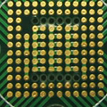
Vias in the pads in high speed PCB
- Vias in the pads in high speed PCB Vias in the pads are useful in high speed designs since they reduce trace length and therefore inductance (i.e. the connection goes straight from pad to plane rather than pad-trace-via-plane)

- Vias in the pads
- bga repair station Shenzhen China
- Vias in the pads
- quick turn-around services
- Vias in the pads
- BGA Electronic Manufacturing SMT House
- Vias in the pads
- bga repair station Shenzhen China
- Vias in the pads
- BGA PCB Assembly Services,
- Vias in the pads
- Ball grid array (BGA) devices rework
- Vias in the pads
- Repair and Warranty Services
- Vias in the pads
- BGA,QFN,0201,0402 part assembly
- Vias in the pads
- X-ray testing, AOI test,function test
Vias in the pads
- VIA IN PAD - WHY AND HOW There are many reasons you shouldn’t use via in pad. It’s not good practice, and those via holes act like BGA via in padlittle capillary straws and suck solder off of the pad or the BGA.
Vias in the pads
- Via in Pads and BGA via-padsIn PCB design, via refers to a pad with a plated hole that connects copper tracks from one layer of the board to other layer(s). High-density multi-layer PCBs may have blind vias, which are visible only on one surface, or buried vias, which are visible on neither, normally referred to as micro vias.
For furhter information, please feel free to contact us, www.pcbsino.com