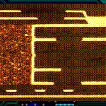
blind and buried pcb, high speed PCB
blind and buried via Multilayer PCB China
Contract manufacturing blind via pcb,
blind and buried via HDI PCB,Shenzhen,
Contract manufacturing blind via pcb,
blind and buried via HDI PCB,Shenzhen,
Blind and buried via solution
-
Blind and buried via solution
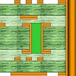
When your design does not allow you to put enough PTH vias due to surface constrains, blind and buried vias might offer you a solution.
- Blind and buried via
- bga repair station Shenzhen China
- BBlind and buried via
- quick turn-around services
- Blind and buried via
- BGA Electronic Manufacturing SMT House
- Blind and buried via
- bga repair station Shenzhen China
- Blind and buried via
- BGA PCB Assembly Services,
- Blind and buried via
- Ball grid array (BGA) devices rework
- Blind and buried via
- Repair and Warranty Services
- Blind and buried via
- BGA,QFN,0201,0402 part assembly
- Blind and buried via
- X-ray testing, AOI test,function test
- Blind and buried via
- BGA Reballing Services
- Blind and buried via
- BGA pcb assembly
- Blind and buried via
- BGA reball rework,repair
Blind and buried via
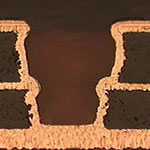
- Blind and buried via A. is a blind via drilled and plated through before pressing the multi layer. To produce this you will need to select the appropriate build up (reverse) and select an extra PTH run in the order details.
Blind and buried via
- Blind Via Hole(BVH) Connect the outermost circuit of the PCB and the adjacent inner layer with plated through-hole, since we cannot see the opposite, so it is called “blind pass”.
For furhter information, please feel free to contact us, www.pcbsino.com