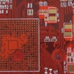
HDI PCB Prototype Multilayer PCB China, blind and buried via
Contract manufacturing of HDI pcb, via in pad, laser drill process
HDI PCB,Shenzhen,China/USA/UK/India/South Africa
High Density Interconnection PCB
-
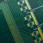
PCBSINO production is fine-tuned to manufacture high technology HDI (High Density Interconnection) PCBs. Products include large and thick HDI boards and also high density thin stacked microvia constructions.
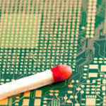
HDI technology enables PCB layout for very high density components like 400um pitch BGA with a high amount of I/O pins. This type component usually requires a PCB board using multiple layer HDI, for example 4+4b+4. PCBSINO have years experience for manufacturing this kind of HDI PCB
FPC PCB |
|
FPC,Flexible PCB,Flex FPC Manufacturer,Fast PCB Prototype |
| FPC Application: |
|
Flexible connector,touch panel...Fast Prototype |
| FPC Thickness: |
|
4 layer,2Layer,1 layer FPC,Flexible PCB,0.05mm-0.4mm |
Flex PCB |
|
FPC, Flexible PCB, Flex FPC Board Fast PCB |
| Flex PCB |
|
Flex PCB/FPC Mass manufacturing, Fabrication |
| Aplication |
|
Medical equipment aplication |
Long FPC |
|
Long Single-layer FPC Flex Flexible PCB with Membrane |
| Application: |
|
Flex PCB Applied for LCD Monitors |
| Treatment |
|
Carbon/Silver Ink Printing or Gold-plated Surface |
Flex PCB |
|
Two Layer Flexible PCB Polyimide Stiffener |
| Stiffener |
|
with Polyimide Stiffener, ENIG Surface Treatment and RoHS Compatible |
| FPC |
|
Carbon/Silver Ink Printing or Gold-plated Surface |
Flexible |
|
MultiLayer Flexible PCB Immersion Silver |
| Treatment |
|
Flexible PCBs with Immersion Silver Surface Treatment |
| Aplication: |
|
LED control boards |
HDI PCB BOARDS (HIGH DENSITY INTERCONNECT)
-
HDI BOARDS (HIGH DENSITY INTERCONNECT)
HDI PCB boards, this is the fastest growing technologies in PCBs, are now available at PCBSINO. HDI Boards contain blind and/or buried vias and sometimes contain microvias of .006 or less in diameter. this will need laser drill, HDI PCB have a higher circuitry density than traditional circuit boards.
There are several types of HDI boards, through vias from top to bottom, with buried vias and through vias, two or more HDI layer with through vias, passive substrate with no electrical connection, coreless construction using layer pairs and alternate constructions of coreless constructions using layer pairs.
HDI Board
High Density Interconnects (HDI) board are a board (PCB) with a higher wiring density per unit area than normal printed circuit boards (PCB). HDI PCB have smaller lines and spaces (<99 µm), smaller vias (<149 µm) and capture pads (<390 µm), I/O>400, and higher connection pad density (>21 pads/sq cm) than employed in conventional PCB technology. HDI board can reduce size and weight, as well as to enhance the whole PCB electrical performance.
Key HDI Benefits
-
Key HDI Benefits
As consumer demands change, so must technology. By using HDI technology, designers now have the option to place more components on both sides of the raw PCB. Multiple via processes, including via in pad and blind via technology, allow designers more PCB real estate to place components that are smaller even closer together. Decreased component size and pitch allow for more I/O in smaller geometries. This means faster transmission of signals and a significant reduction in signal loss and crossing delays
HDI construction types
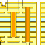
The object of HDI is to achieve higher wiring density than conventional boards, and a central feature of the technology is the microvia, blind vias defined by hole diameters smaller than150µm and normally drilled by laser. The microvia only extends between two, or at most tree layers, and is usually used in combination with buried vias and regular conventional through-hole vias. A prime example of HDI technology is the BGA package itself which is a printed circuit board with extremely small features.
While the fabrication of conventional PCBs are standardized and well known, HDI boards are constructed in a wide variety of ways. IPC’s sectional design standard for HDI (IPC-2226) details 6 general classes of construction from class I where microvias are formed in the surface of a conventional PCB, to type VI in which electrical interconnections and mechanical structure are formed simultaneously. One of the prevalent structures, type III, is shown in the illustration to the right.
Via in Pad Process
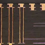
Inspiration from surface mount technologies from the late 1980's has pushed the limits with BGA's, COB and CSP into smaller square surface inches. The via in pad process allows for vias to be placed within the surface of the flat lands. The via is plated and filled with either conductive or non-conductive epoxy then capped and plated over, making it virtually invisible.
this Sounds simple but there is an average of eight additional steps to complete this unique process. Specialty equipment and trained technicians follow the process closely to achieve the perfect hidden via.
HDI(High Density Interconnection)
High-density interconnection (HDI) substrates have high-density circuits that make it possible for electronic parts mounted on a PCB to send and recieve electrical signals between themselves. The products are used for mounting the main parts of mobile devices and transmitting their signals.
HDI(High Density Interconnection)
HDI(High Density Interconnection)
HDI(High Density Interconnection)
1 / 3
General Features
Improves the performance of products because of high integration
Makes it easier to automate the assembly of PCBs
Reduces total costs
Standard or First Generation Microvias
Create routing density (eliminate through vias)
Reduce layer count
Enhance electrical characteristics
Standard Microvias limited to layers 1 - 2 & 1 - 3
Stacked MicroVias (SMV®) or Second Generation Microvias
Allows increased routing on multiple layers
Provides routing solutions for next generation applications
1 mm - 0.8 mm - 0.65 mm - 0.5 mm - 0.4 mm - 0.3 mm & 0.25 mm
Provides solid copper plate eliminating potential solder voiding
Provides a Thermal Management Solution
Improves Current Carrying Capability
Improves Current Carrying Capability
Provides a Planar surface for BGA (Via-in-Pad)
Allows any layer via technology
Deep Microvias (DpMV™)
Provide additional dielectric material & small geometry features.
Improved Impedance performance
Provides RF Microvia solutions
Provides a solid copper plate
Improves Current Carrying Capability & Thermal Management
Provides a Planar surface for BGA (Via-in-Pad)
Deep Stacked MicroVias (DpSMV™)
Provides additional dielectric for RF applications
Maintains small geometries on multiple layers
Improved signal integrity
Provides a solid copper plate
Improves Current Carrying Capability & Thermal Management
Provides a Planar surface for BGA (Via-in-Pad)
Any layer HDI
Multilayer copper filled stacked micro via structure
1.2/1.2 mil line/space
4/8 mil laser via capture pad size
Material options:
High temperature FR4
Halogen - Free
High Speed (low loss)
High Density Interconnect(HDI) PCB Fabrication
-
High Density Interconnect(HDI) PCB Fabrication
What are High Density Interconnector (HDI) Printed Circuit Board (PCBs)? What are the current limits of Bittele Electronics’ HDI PCB fabrication capability? What new capabilities are planned in the future? PCBSINO at Bittele Electronics have improved and upgraded our manufacturing facilities in 2016 to include HDI board fabrication and assembly. PCBSINO now provide manufacturing High Density Interconnect(HDI) PCB service in our comprehensive list of PCB fabrication and assembly capabilities.
High Density Interconnect PCB (HDI)
High Density Interconnect PCBs have a higher wiring density per unit area than conventional PCBs and are utilized in complex small form factor designs. High Density Interconnect PCB (HDI PCB) helps reduce size and weight, as well as enhances electrical performance of a device.
Fine Line PCB
8 Layer Flip Chip - HDI PCB
8 Layer Flip Chip
Benefits of HDI PCB Technology with Micro Circuits:
Shorter PCB manufacturing lead times and improved device performance for Flip Chip, BGA, MCM, SIP technologies and medical devices.
Allows utilization of technologies that require ultra thin cores, fine line geometries and alternative via technologies for enhanced thermal transfer in the case of a thermal PCB.
Allows utilization of the technologies that require 20um circuit geometries, 30um dielectric layers, 50um laser vias and 125um bump pitch processing.
Laser Drill Technology
Drilling the smallest of micro-vias allows for more technology on the board's surface. Using a beam of light 20 microns (1 Mil) in diameter, this high influence beam can cut through metal and glass creating the tiny via hole. New products exist such as uniform glass materials that are a low loss laminate and low dielectric constant. These materials have higher heat resistance for lead free assembly and allow for the smaller holes to be used.
For furhter information, please feel free to contact us, www.pcbsino.com
