Contract manufacturing of HDI pcb, volume
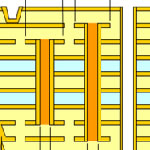
blind and buried via, via in pad, laser drill
-
PCBSINO production is fine-tuned to manufacture high technology HDI (High Density Interconnection) PCBs.
Products include large and thick HDI boards and also high density thin stacked microvia constructions.
- HDI PCB manufacturing:
- Prototyping of HDI PCB
- HDI PCB manufacturing:
- Low cost HDI PCB
- HDI PCB manufacturing:
- HDI PCB fabrication Shenzhen China
- HDI PCB manufacturing:
- Fast HDI PCB fabrication
- HDI PCB manufacturing:
- impedance control, Fabrication
- HDI PCB manufacturing:
- High frequency HDI PCB
- HDI PCB manufacturing:
- Multilayer HDI PCB Manufacturing
- HDI PCB manufacturing:
- blind/buried via hdi PCB fabrication
- HDI PCB manufacturing:
- Carbon/Silver Ink Printing or Gold-plated Surface
-
Key HDI Benefits
Improves the performance of products because of high integration
Makes it easier to automate the assembly of PCBs
Reduces total costs
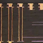
Standard or First Generation Microvias
Create routing density (eliminate through vias)
Reduce layer count
Enhance electrical characteristics
-
Laser Drill Technology
Drilling the smallest of micro-vias allows for more technology on the board's surface. Using a beam of light 20 microns (1 Mil) in diameter, this high influence beam can cut through metal and glass creating the tiny via hole.
For furhter information, please feel free to contact us, www.pcbsino.com