 High Speed PCB Layout |
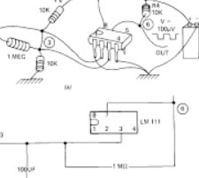 Schematic from sketch |
 Quick turn PCB layout |
 PADs PCB layout |
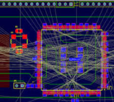
 Cadence Capture PCB layout |
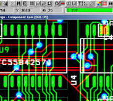
 Altium PCB layout |
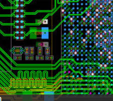
 High speed PCB layout |
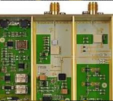 RF PCB layout |
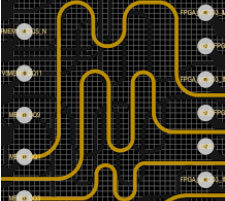
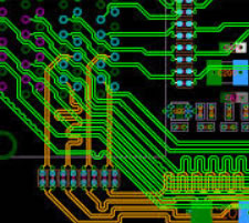 Differential Pair PCB layout |
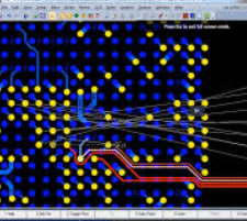
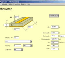 Impedance control PCB layout |
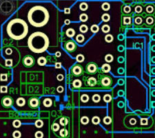
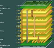 Multi-Layer PCB layout |
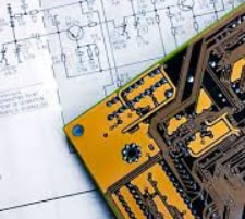 Schematic double check |
For furhter information, please feel free to contact us, www.pcbsino.com
 English
 Español
 Português
 Deutsch
 Français
 Italiano
 Россия
 Türkçe
 Polski
 대한민국
대한민국
 بالعربية
 فارسی
فارسی
 Dutch
Dutch
 Afrikaans