Countersink hole PCB manufacturer China, PCB prototype
Contract manufacturing of countersink hole pcb, Mass Production,
Low cost countersink hole PCB,Shenzhen,China/USA/UK/India/South Africa
Countersink hole |
|
Countersink hole PCB Manufacturing |
| Countersink hole |
|
PCB prototype |
| sink hole |
|
Countersink hole PCB manufacturer China, |
Countersink hole |
|
Contract manufacturing of countersink hole pcb, |
| Countersink hole |
|
Low cost countersink hole PCB, |
| sink hole |
|
Shenzhen,China/USA/UK/India/South Africa |
Countersink hole |
|
Countersink hole PCB manufacturer China, |
| Countersink hole |
|
PCBs with Immersion Silver/Gold Surface Treatment |
| sink hole |
|
Countersink hole PCB Manufacturing |
Countersink Hole PCB
-
Countersink Hole PCB
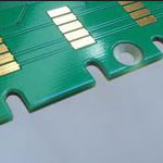
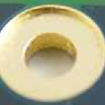
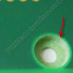
A conical hole which is cut to allow the flat head screw to be used is called a countersink hole. It can also be called as a conical hole that is cut into a PCB laminate, or a hole created by using a drill. The main purpose is to let the head of a countersunk screw, once it is inserted and screwed down in the hole, to sit flush with the surface of the laminate. The cone shaped hole, which is cut into the PCB laminate, is a countersink. It is generally used to permit the tapered head of a screw to sit flush with the top or bottom of the laminate.
Countersink
A countersink is a cone shaped hole cut into the laminate. It is typically used to allow the tapered head of a screw to sit flush with the top of the laminate. By comparison, a counterbore makes a flat-bottomed hole and its sides are drilled straight down. This is usually used to fit a hex-headed cap or screw.
To accurately drill your countersunk holes, we will need the following information.
Angle of the drill
Major Diameter (finished diameter of the hole at the surface)
Depth the countersink is to be drilled
On which side of the board is the sink? Top or Bottom?
The finished diameter of the shaft of the hole
Is the sink and shaft to be plated or non-plated?
What is a Countersink Hole & How to Use it on PCB Pads
Many people are perplexed by countersink holes (often called sink hole or countersunk hole) on PCB boards. Indeed these terms deserve a good explanation.
A countersunk hole is simply a normal right cylindrical through-hole with an additional right conical section removed on the top. The cone angle is typically 82 or 100 degrees. A related term is counterbore hole which has an additional flat-bottomed hole. The following are two cross-section diagrams, courtesy of Wikipedia.
Countersunk holes What is a Countersink Hole & How to Use it on PCB Pads
Cross-sections of countersink holes of various chamfer angles
Counterbore Cross Section What is a Countersink Hole & How to Use it on PCB Pads
A cross-sectional diagram of a counterbore hole
On a PCB pad, countersink or counterbore holes can be plated for unplated.
A common usage of countersink or counterbore holes is to allow the head of a countersunk bolt or screw, when placed in the hole, to sit flush with or below the surface of the surrounding material.
Countersink Hole is used in PCB board that sink the screw head into PCB laminate.so that the board looks clean and flat.countersink hole generally have two types of shapes.V figure Count-sink and T figure Count-Sink.
PCB Countersink hole
-
PCB Countersink hole
When you plan to design countersink in your board, below information is required:
Which side of countersink hole be drilled? Like Bottom Layer?
Is the countersink hole plated or non-plated?
What is countersink hole diameter(d2)?
What is through hole diameter(d1)?
What is the depth of countersink hole need to sink(t1)?
What is angle of countersink hole(like 90 degree or other)?
PCB with countersink holes
Countersink Holes is for fix the PCB onto/into the plastics BOX by the screw.
Many people called countersink holes as sink hole or countersunk hole on PCB boards.
is there any option to create countersink in the Allegro tool, (If anybody knows, please share it.)
I normally mention the countersink details in the drill chart for the starting drill diameter & the Fabricators are able to do it correctly.
We use it for Aluminium metal PCBs in the Mounting holes to get a better contact with screws (Ground_signal Bonding).If they get a separate drawing, they have to digitize it and edit the needed NC drill files manually, but this takes time and money.
A Gerber file is data for photoplotters, but not for NC drill machines. The board house may transform a Gerber file into the needed NC drill file, but this is a manual process using their CAM CAD system and will take some time again.
A separate NC drill file for the countersunk holes only will be the best data for them, but you should discuss the details with them.
countersink holes require additional drill jobs
-
countersink holes require additional drill jobs
But you should be aware that countersunk holes will require additional drill jobs for the PCB, especially if both sides are countersunked. Drilling two or three boards together in a stack as usual is not possible for the countersunks, each board must be drilled separately. If you want to reduce costs, try to avoid countersunks if possible.
METHOD 1.
Place a pad on the PCB, set hole size to 2.4mm and annular ring size to less than 2.4mm.
problems:
-if you set annular ring to 0mm you will get manufacturer errors, as you will get a virtual 0mm point surrounded by soldermask clearance ring in gerber files
-if you set annular ring to 2.4mm, same as hole size, you will get a hole with soldermask clearance ring (makes the soldermask susceptible to peeling with screw torque)
-using a PCB template rules from http://www.eurocircuits.com/Altium-Designer-templates-with-Eurocircuits-design-rules (my fabricator of choice) for Class 6C - 2 layer - 1.55 mm i get an design rule error saying "Hole Size Constraint (Min=0.25mm) (Max=2mm) (All) 4" which means they do holes up to 2mm. Clearly that can not include routing and cutouts. What gives? How do I make a larger hole then?
METHOD 2.
Create a PCB library footprint for the hole (also from a pad). The bonus is that you can add a 3d model of the screw [SEE ATTACHED IMAGE], which makes it much nicer for the final board 3D render. You could add a 3D model to each screw hole in the METHOD 1, but you would have to align it one by one, and here its all pre-done.
problems:
-this METHOD gives errors when processing the PCB as it is an object in the PCB not referenced in the schematic
-I also tried creating a schematic library part, and adding the above mentioned PCB library footprint(pad) and 3D model to it - now I had to hide unnecessary bloat items in the schematic
-same Eurocircuits fabricator problem as above
METHOD 3.
Place a primitive/polygon on a mechanical layer and perform [SEE ATTACHED IMAGE] TOOLS>CONVERT>CREATE BOARD CUTOUT FROM SELECTED PRIMITIVES
problems:
-there is no nice screw model representation like in METHOD 2
-will it generate proper gerber drill data to the manufacturer? I am afraid it will be just a random cutout that they will have to route in some expensive way
-I don't get the nice dimension outlines: screw head (grey circle) and screw clearance (green circle)
-it will not make a plated hole: I have read that its best to keep all holes plated, even mounting ones, as it reduces the tooling overhead. Is that true?
For furhter information, please feel free to contact us, www.pcbsino.com


