Protel 99 SE PCB layout design tools
China PCB Manufacturing, Shenzhen PCB Manufacturer, Making Circuit boards
PCB Contract manufacturer, PCB Fabrication, Turnkey assembly services
Buy Print circuit board, customer: /USA/UK/Canada/South Africa...
PCB Supplier Shenzhen, China, PCB Manufacturer, Turnkey services
-
PCBSINO is the Top 5 PCB manufacturer company in China.
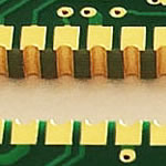
PCBSINO do rapid Prototype within 24 hours. we can make Flexible Print circuit boards and Rigid circuit boards, like FR4, High TG FR4, Rogers 4003, 4350,Al Aluminum metal Core MCPCB, Al2O3 Ceramic,Taconic,Halogen Free material, CEM-3, Fr2, CEM-1, CEM-2, 94VO, Rogers HF material, Polymide,Flexible PCB FPC etc.
we already made many type electronic product for our customer, Our turkey services team can source original components part for your project, senior Electronic engineer will follow each step of the production and do function test in PCB house.
Express PCB |
|
Rigid PCB Rapid Prototype,24 hours |
| Fr4 PCB |
|
prototype Lower to 15USD ! |
| Rapid Prototype |
|
Fr4 Rigid PCB Rapid Prototype China, |
Turnkey Services |
|
Turnkey PCB Assembly Services, |
| Turnkey services |
|
Print circuit board Manufacturing, Turnkey Services |
| Turnkey Assembly |
|
Through Hole PCB components wave soldering Assembly |
Protel 99 SE PCB layout design tools
-
free download! no time limit…
Protel 99 SE PCB layout design tools
Protel 99SE
Protel 99 SE schematic and PCB design tutorial (3rd edition)
POWERFUL TOOLS FOR
NEXT-GENERATION ELECTRONICS DESIGN
Altium software empowers makers, engineers, and designers of electronics-based products
to create a smarter, safer, and more connected world.
Well Protel is a very good tool for the PCB designing here I am going to post a introduction and basic function tutorial for you people after this tutorial you will be familiar with the PROTEL.
There are Main Three Parts when you are going to design a PCB
1.[FONT="] [/FONT]Schematic Design.
2.[FONT="] [/FONT]Add Footprints
3.[FONT="] [/FONT]PCB artwork
Schematic Design: in this section you have to draw the interactive Circuit diagram.
Footprints: as you are going to Draw the layout of the PCB you must be aware with the Component size and according to that you have to place the outline of the particular component.
PCB artwork: in this section you have to decide the place or the components and also draw a connection line between components
We will see all this section in detail first of lets Start form scratch.
Make a New File:
Remember that .ddb is the extension for the Protel file
PROTEL SCHEMATIC CAPTURE & PCB LAYOUT
2/07/02, 2/11/02 Prof. M. Heller
CREATE A NEW DESIGN DATABASE
- File, New Design
- Set Design Storage Type: Select, MS Access Database
- Database File Name: Type in you Product Name
- Click OK
CREATE SCHEMATIC DOCUMENT
- Click on your Document Folder in your database
- File, New, Click on Schematic Document
- In the New Document dialog, Click on Schematic Document
- Click OK
- Select Edit, Rename to change the filename (do not change the extension)
- Set styles: Dbl Click on the new schematic, select Design, Options, select Sheet Options tab, set style under Standard Style and set orientation
- Set general preference: Select Tools, Preferences, select Default Primitives tab, enable Permanent (on the right side)
- Save schematic: Select File, Save
- Fill screen: Select View and Fit Document
FIND A SCHEMATIC COMPONENT
- Select Tools, Find Component produces the Find Schematic Component Dialog: If you know a few characters of the part like a 4011 nand IC, enable By Library Reference and put in *4011* and click Find Now. Libraries that contain that part will be listed. Add the library to your list by highlighting the library that you want to add and the by clicking Add Library to List and close the Find Component Dialog.
- If part is already in a library in your library list, click Browse Schematic tab on the left of your screen. Click on the part library of interest and put in * the Filter window and Enter. You can scroll down the list of parts in that library. If you are looking for capacitors, put in *cap* in the Filter window and enter. Various capacitor forms will be listed. Click on the part and you can see its general shape in the window below the parts list.
- Select Tools, Find Component produces the Find Schematic Component Dialog: If you are looking for more generic parts like capacitors, connectors, and resistors, enable By Description and put in connector, for example, and click Find Now. Libraries that contain that part will be listed. Add the library to your list by highlighting the library that you want to add and the by clicking Add Library to List and close the Find Component Dialog. You will need the BJT.Lib and the Simulation Symbols.Lib in the SIM.ddb for the Protel Tutorial.
CREATING YOUR OWN SCHEMATIC LIBRARY
Some parts are not in the Protel Libraries. There are two Libraries - Schematic and PCB. You can create your own Schematic and PCB libraries within your Design Data Base. Once you have done this you can copy parts from other schematic libraries to your schematic library and edit it. Or you can copy parts from other PCB Libraries to your PCB library and edit it. You can use the same footprint of the copied part, use a different footprint in the Pcb Footprint Libraries or create a new Footprint. You probably can find a footprint in the Pcb Footprint Libraries that is close enough so that you can modify it, as necessary. Remember, you need to specify a footprint in the Attributes of each part. You can now open up the footprint libraries to find the Footprint for the part: Select Files, Open, C:/Program Files/Design Explorer 99 SE/Pcb. You will see a Connectors, Generic Footprints, or IPC Footprints Folder in this PCB folder. Open the folder of interest and Dbl-Click on the xxxx.ddb of interest and that PCB (Footprint) Library is added to you ddb. Click on the Browse PCBLib tab. You now can scroll through the Footprints or use the mask which is a search function to find the footprint of interest. (This is where we got the resistor and capacitor footprint names).
- To create a new schematic library, first open or create a design database in which to store the library.
- To create a new schematic library, from within a design database select File New, and double click on the SchLib icon in the New Document dialog. A new empty schematic library document will be created in the current folder of the design database. To open the library, double-click on its icon in the design window, or click on its icon in the navigation tree.
- As a library is a set of components, it cannot exist without at least one component. When you create a new library, an empty component sheet (called Component_1) is also created within the library. To rename Component_1 with a name of your choice, open the library, select Component_1 from the list in the schematic library editor panel, and select Tools Rename Component from the menus.
- Schematic components can be copied within a library, or copied or moved between libraries in a design database.
Exporting the schematics for PCB design?
I have completed the schematics and am trying to hand it over to the manufacturer for PCB design and assembly. They use Protel 99se and am asking if I can export my schematics that would be able to be imported into the Protel.
I have searched the community for help but only found those around exporting a PCB design, which I have NOT done yet and have every intent to pass to our manufacturer to perform this function.
Has anyone done this before and what file format and process did you use to achieve this?
Any help or pointer would be appreciated. Thank you in advance.
Typically you send the board house gerbers for manufacturing and a BOM/pick and place list for assembly. Are you sure they need to open your design in Protel99se? Even if they did need to manipulate the design, that's a bit of an odd request for format considering it's a 15+ year old version that doesn't run on modern OSes.
However, I think the way this is supposed to work is that you download your design as a JSON file (through the list of export options), then use the upverter converter script21 to go to Altium (Protel) format. I honestly don't think this tool is working or up to date though. I would love to be corrected on the current status of conversions though.
This post might also help you out:
PCB Design : protel(altium) to Allegro pcb design
PCB Design Forums
protel(altium) to Allegro pcb design
Started by archive on 21 Aug 2007 4:09 AM. Topic has 11 replies and 38661 views.
Last post on 17 Apr 2012 5:16 AM by Dan646.
Hy everyboby!! I was wondering if could some one help me. I has a board on the protel(altium) format, but i have to route this board on the Allegro pcb design. is it possible??
Originally posted in cdnusers.org by vanilson
archive archive
*** Firstly you must save Protel pcb file as Protel PCB 2.8 Ascii. (Save as --> Export to Protel PCB 2.8 Ascii) Then,
you can import this file in Orcad Layout. (Import -->Protel PCB) Now you have .max file. Lastly. you must use
Orcad Layout to Allegro Conversion Program. (max to brd file conversion)
BlueCad
Originally posted in cdnusers.org by bluecad
Design Printed Circuit Board By Protel 99se
Most designs today are built on Printed Circuit Boards (PCBs), which consist of multiple layers of electrical copper and insulating material sandwiched together. Several Electronic Design Applications (EDA) exist to both create schematics of a circuit and transfer them to a working PCB layout. At the University of Florida, we have access to Protel 99SE for these functions. The resulting PCB design can then be sent to a company for a professional board with silkscreens, multiple layers, etc. MIL also has the ability, through a T-Tech Quick Circuit, to make single and double sided circuit boards PCBs out of copper-plated sheets of insulating material. The latter process is unable to make complicated designs, but it both quick and cheap. This tutorial covers the creation of a sample design using Protel 99SE, and its preparation to be milled out by the T-Tech.
First we must create an overall database that will contain all the individual components of the design – the Schematics that describe the circuit, the Printed circuit board Designs that physically layout the components and their connections, and other assorted files.
PCB Design Engineer at Behr-Hella Thermocontrol (BHTC)
Behr-Hella Thermocontrol (BHTC) North Maharashtra University
H Start Protel and select File/New. Use a MS Access Database and give it a name – this will create a Design Database file (extension .DDB) that contains all the parts of your design. In this case, we’ll call it Tutorial.DDB. Maximize the window – it makes it easier to have one title bar.
H The Database has its own internal File System – go into the Documents Folder, select File/New and create a new Schematic Document. Always rename your files to something more descriptive (HC11 IO.sch, Power Regulation.sch, etc.) – this will make it easier to keep track of what information is in each document. We’ll stick to the pattern and call it Tutorial.sch.
H Save often – both Windows and Protel can be buggy at times, and the last thing you want to do is lose over an hours work because of a crash.
Designing of the PCB layout as per the requirement.
Creating schematic circuit usingOrcad CAPTURE.
Manage component library, Creation new component in schematic & footprint.
Schematic netlist creation, component placement, routing.
Creation of production and assembly output files (GERBER, DXF or Pick & Place data).
Verify & check Gerber data in CAM350 software.
Designing layout for LED Drivers & ballast with compact & different PCB Size.
Experience of working with design constraints for Hi-Speed digital and analogue routing.
Prepare & follow design guidelines as per IPC standards.
Give PCB design training to new engineers.
Guiding the PCB Layout Design Engineer during placement, Routing.
Coordinating with Hardware Engineer while doing component placement, critical track routing.
Coordinate with Mechanical designer for mechanical BOX.
Communicate with PCB manufacturer for PCB related queries and require help.
Prepare document with respect to ISO standards.
Experience of working to project timelines
First of all, thank you for the Answer. Where i can download the Orcad Layout to Allegro Conversion Program? I am using the Allegro PCB editor 15.5.
Trusting in your help again,
Vanilson
Originally posted in cdnusers.org by vanilson
archive archive
Cadence has a translator that takes the .MAX file and will convert it to a .BRD file. Works pretty well.
Last time I downloaded it from: www.orcad.com/community.layout.dl.aspx (look near the bottom of the page).
I hope you can still find it.
Originally posted in by cadpro2k
MAKING GUIDE Protel 99 SE PCB DESIGN USING EXPLORER
OPENING EARLY STEP Protel 99 SE
1.1 Initial steps to open protel 99 SE
Once the installation is complete we do, a subsequent step is an introduction to the software, so we did not encounter any significant obstacles at work in the process. The introduction of software here we emphasize brief introduction Protel 99 SE how to open, create a new database, create a new file.
First we open the first software Protel 99 SE by clicking Start ► Programs ► ► Protel 99 SE Protel 99 SE, then the appearance of Protel 99 SE or less as shown in the picture below :
Protel display a blank worksheet as shown in the figure above, before we start, from the above worksheet we will create a new database that will be used to design Schematic diagram to be a PCB, how to create a new database in the following way:
Click the File menu ► New, as shown in the figure below. It will display the New Design Database dialog box as shown in the figure below.
Fill the box with Design Storage Type "MS Access databese" and name the Database File Name "MyDesignCAD" and specify the Location Database by clicking Browse, as shown in the figure below, when finished click OK.
Design Explorer it will display as shown below , this is where we will make various types of files that are related to each other to form a database that is implemented on a desing and layout components . The next step after we know how to open protel is how we create a new file sebuat that will serve as editor - at each step TIPA performing tasks that we do . First we will create a file Schematic Diagram which we will use to draw the series which will we make as a PCB , the steps are as follows . Right click on any empty space in the area , it will display the menu as shown in the figure below , then click the New menu .
Once we select the New menu it will display a dialog box to confirm us to choose the type of file that will be created , as shown below , select the " Document Schematic " and continue by selecting OK
.
Document menu will appear as shown in the figure below, the Document menu will appear an icon of the file we have created, name the file with the name "Schematic Diagrams" and continue by pressing Enter, after that proceed to Double click on the icon is to open the worksheet Schematic Diagram, it will be displayed on the worksheet approximately Schematic Diagram drawn as shown below
To display the types and kinds of components that we will use later click the Browse menu, it will display a menu of components as shown in the figure below
I would be more than happy to look over your design and provide feedback from a manufacturer's perspective. kindly provide the Upverter project link or email me the gerbers, BOM, etc.
Happy new year!
Hooman Javdan
VP, Circuits Central Inc
416.285.5550 x 229
aShireDukeJan '16
I had a similar experience. When I had the board assembled they asked for either v2.8 Protel or ascii cad files in addition to the gerber, BOM, and SMT files. They explained that the protel/ascii files were required to provide shape/polarity information that the gerbers do not provide.
-- Open the schematic library you wish to copy the component from and select the component in the Components list in the schematic library editor panel.
-- Select the part that you want to copy. Select Edit, Select ALL then copy.
-- Open your library by clicking on it via the Explorer tab. Select Tools then New Component. Change the Component Name in the dialog box and click OK.
-- Click Description on the Browse SchLib tab. Put the footprint you want into the Footprint 1 slot. Close the library if you are finished.
- Create your own schematic part by using the drawing tools or modifying a copied schematic part.
-- Open your schematic library and select the part you want to modify or Select Tools then New Component. Change the Component Name in the dialog box and click OK.
-- Use the drawing tool to create or modify the part.
-- Click Description on the Browse SchLib tab. Put the footprint you want into the Footprint 1 slot. Close the library if you are finished.
PLACING PARTS ON THE SCHEMATIC
- Highlight the Part and click on the Place button. The part now floats with the cross hairs.
For furhter information, please feel free to contact us, www.pcbsino.com