KiCAD PCB design layout tools
China PCB Manufacturing, Shenzhen PCB Manufacturer, Making Circuit boards
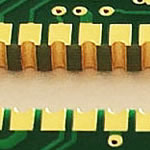
PCB Contract manufacturer, PCB Fabrication, Turnkey assembly services
Buy Print circuit board, customer: /USA/UK/Canada/South Africa...
KiCAD PCB design layout tools
-
free download! no time limit…
KiCAD PCB design layout tools
KiCad EDA
A Cross Platform and Open Source Electronics Design Automation Suite
DOCS DOWNLOAD
Schematic Capture
With the schematic editor you can create your design without limit; there are no paywalls to unlock features. An official library for schematic symbols and a built-in schematic symbol editor help you get started quickly with your designs.
LEARN MORE
KiCad
From Wikipedia, the free encyclopedia
KiCad
KiCad-Logo.svg
KiCad Layout Editor
KiCad Layout Editor
Original author(s) Jean-Pierre Charras
Developer(s) KiCad developers[1]
Initial release 1992; 25 years ago[2]
Stable release
4.0.6[3] / March 7, 2017; 5 months ago
Repository git.launchpad.net/kicad
Written in C++[4]
Operating system Windows, macOS, Linux, FreeBSD
Available in 8 languages[citation needed]
Type EDA
License GNU GPL v3+[5]
Website www.kicad-pcb.org
KiCad Eeschema for Schematic capture.
KiCad Pcbnew for layout design.
KiCad 3D Viewer showing both VRML and IDF features on a demo board.
KiCad 3D Viewer
KiCad is a free software suite for electronic design automation (EDA). It facilitates the design of schematics for electronic circuits and their conversion to PCB designs. KiCad was originally developed by Jean-Pierre Charras, and features an integrated environment for schematic capture and PCB layout design. Tools exist within the package to create a bill of materials, artwork, Gerber files, and 3D views of the PCB and its components. KiCad's popularity is fueled by its GerbView component, used as Gerber viewer by users of other EDA software that does not support this feature such as CircuitMaker. Olimex has announced to have switched from EAGLE to KiCad as their primary EDA tool.
kicad-library
The schematic and 3D libraries supported by KiCad team. Note that the footprint libraries are the *.pretty repos themselves.
packages3D
3D models for rendering and MCAD integration
kicad-library-utils
Some scripts for helping with library development
Python
Search repositories…
Type: All Language: All
kicad-source-mirror
A mirror of the KiCad development branch, which is hosted at launchpad (updated every time something is pushed). Pull requests on github are not accepted or watched.
kicad-library
The schematic and 3D libraries supported by KiCad team. Note that the footprint libraries are the *.pretty repos themselves.
CMakeModules Add 'make uninstall' support using CMake. Typically must be run as ro…
library Merge pull request #1557 from Misca1234/TSL2550
modules Merge pull request #1557 from Misca1234/TSL2550
template Fix environment variable used in default symbol library table.
.gitattributes Fixes for .gitattributesfiel
.gitignore Ignore /internat/ directory
.travis.yml Good to go (#3) 6 months ago
CMakeLists.txt Removed KICAD_DATA dir which is redundant on OSX and changed the pref…
CONTRIBUTING.md updating and renaming CONTRIBUTING file
COPYRIGHT.txt Add license info for libraries (the GPL license)
README.md Update README.md
library-check.sh Fixed accidental removal of douille
Incorrect component models in 3D viewer?
I have found the 3D viewer quite useful. On my first board it saved me from having 3 terminal block connectors the wrong way round. It's worked fine for my last 3 boards apart from some components not appearing to have… read more
Welcome to the KiCad.info Forums!
This is the forums of KiCad.info, which intends to be the premier source of information about KiCad and the best place to discuss KiCad. As with other forums and online resources, we hope you will be diligent in searchin
This is a short and fast introductory video for those interested in getting started using KiCAD. I wanted to demonstrate a basic work-flow through schematic capture and PCB layout modules, instead of touching on every function or element of the user interface.
Printed Circuit Boards (PCB) are the heart of any electronic device, from toasters to smartphones. But so far, the engineers who design the boards often have had no option but to use proprietary tools. That's about to change: CERN experts are adapting the open-source software KiCad to make it an efficient tool for designing open-source hardware. This free software makes it easier for electronics engineers to share their designs.
KiCad development began in 1992. The software – which runs on the computer-operating systems GNU/Linux, Windows and Apple OS X - creates schematics for printed circuit boards with up to 32 copper layers with additional technical layers. Since 2013, experts in the CERN Beams department have made important contributions to KiCad (link is external) as part of the Open Hardware Initiative (OHI), which provides a framework to facilitate knowledge exchange across the electronic design community. “Our vision is to allow the hardware developers to share as easily as their software colleagues,” says Javier Serrano, head of the BE-CO-HT section and OHI initiator. “Software sources are easily shared online because they are text files and everyone has access to editors and compilers that turn the sources into a program. On the other hand, in the case of hardware design, most of the time this is done using proprietary tools. Therefore, in order for people to modify the sources, they need to use those proprietary tools.”
KiCad is a set of applications used to capture electronic schematics and design printed circuit boards. KiCad runs on Windows, Linux, and Apple OSX and is released under the open source GNU GPL.
Please note that this is the KiCad developers website. If you have a user related question, please use one of the KiCad user resources listed in the "Community" section of the KiCad website http://kicad-pcb.org/.
If you wish to contribute to KiCad see the Developers section in the KiCad website at http://kicad-pcb.org/contribute/developers/.
Useful links
‾‾‾‾‾‾‾‾‾‾‾
Main website:
http://kicad-pcb.org
Users mailing list:
http://tech.groups.yahoo.com/group/kicad-users/
Developers mailing list:
http://launchpad.net/~kicad-developers
#1538510 Segfault add exist sheetlist
KiCad 16
CRITICAL FIX COMMITTED
#1553804 Segmentation fault (core dumped) while re-drawing traces
KiCad 38
CRITICAL FIX COMMITTED
#1579042 pcbnew and footprint editor crashes when starting
KiCad 20
CRITICAL FIX COMMITTED
The KiCad project aims at creating a portable, cross-platform, Free/Libre/
Open-Source EDA Suite, capable of schematic and printed circuit board
design. The suite consist of a project manager, schematic editor,
netlist converter, pcb designer and a gerber viewer.
There are separate SlackBuilds for the libraries and additional
documentation, kicad-library and kicad-doc.
#1635266 Unhandeled exception class: St9bad_alloc what: std::bad_alloc
KiCad 6
CRITICAL FIX COMMITTED
#1647803 Pcbnew crash when updating netlist.
KiCad 10
CRITICAL FIX COMMITTED
#1649597 foorprint editor crash by draw line and "escap" key
KiCad 6
CRITICAL FIX COMMITTED
#1653146 Assertion failed when trying to delete track with router tool active
KiCad 6
CRITICAL FIX COMMITTED
#1655858 Pcbnew crashes on exit in Opengl mode when a footprint on the board was edited in the fp editor
KiCad 12
Code repository (contributions are welcome):
https://code.launchpad.net/kicad
Official footprint repositories (contributions are welcome):
http://github.com/KiCAD (all repositories with '.pretty' suffix)
Official schematic parts and 3D models library repository:
https://github.com/KiCad/kicad-library
Library developers mailing list:
https://launchpad.net/~kicad-lib-committers
Official documentation repository:
https://github.com/KiCad/kicad-doc
Documentation team mailing list:
Screenshot from KiCad of a design for a printed circuit board (Image: KiCad)
When the KiCAD project started at CERN, many free tools were already available to hardware designers but none was easy enough to use when designing a complex circuit. Among them, KiCad showed the best potential. “We started by cleaning the basic code and introducing a new graphical engine,” says Tomasz Wlostowski, a member of the BE-CO-HT section who, among other things, is in charge of supervising the development of new features for KiCad. “With our contribution, we aim to develop KiCad up to a point where it becomes the de facto standard for sharing, and more and more users, including corporate ones, start working with it.”
Printed Circuit Boards (PCB) are the heart of any electronic device, from toasters to smartphones. But so far, the engineers who design the boards often have had no option but to use proprietary tools. That's about to change: CERN experts are adapting the open-source software KiCad to make it an efficient tool for designing open-source hardware. This free software makes it easier for electronics engineers to share their designs.
KiCad development began in 1992. The software – which runs on the computer-operating systems GNU/Linux, Windows and Apple OS X - creates schematics for printed circuit boards with up to 32 copper layers with additional technical layers. Since 2013, experts in the CERN Beams department have made important contributions to KiCad (link is external) as part of the Open Hardware Initiative (OHI), which provides a framework to facilitate knowledge exchange across the electronic design community. “Our vision is to allow the hardware developers to share as easily as their software colleagues,” says Javier Serrano, head of the BE-CO-HT section and OHI initiator. “Software sources are easily shared online because they are text files and everyone has access to editors and compilers that turn the sources into a program. On the other hand, in the case of hardware design, most of the time this is done using proprietary tools. Therefore, in order for people to modify the sources, they need to use those proprietary tools.”
Going from Schematic to PCB Layout in KiCad (using Cvpcb)
NOTE: This tutorial was written in 1847, and kicad has changed a lot since then! Check out this awesome free kicad video series tutorial from Contextual Electronics for a more up-to-date version. They also have a small course on building your first pcb that includes everything from circuit board design in kicad to manufacturing the pcb.
This section will explain the process of going from the schematic to pcb layout in KiCad. The process is a little bit more involved than in Eagle, and requires 4 steps:
First, make sure all components are annotated (numbered).
Generate a netlist that contains all the components and their connections.
Use cvpcb to assign pcb footprints to all the components (not necessary if new components have not been added.)
Load the netlist in pcbnew.
Kicad Tutorial: PCB edges
by Layne on February 26, 2013
This is part of a series of short tutorials on advanced topics of using Kicad, the favorite schematic/PCB design software here at Wayne and Layne.
An important part of designing a PCB is to clearly indicate the outline of the board, so the board house will know how to cut your boards apart. Most PCBs are rectangular, but sometimes you want to add a more complex outline (like a circle or hexagon) or a very complex outline (like the PCB for the Video Game Shield, shown below).
vgs_complex
To make it easier to determine where the PCB edges should be, you probably watch to switch your cursor to be the full-screen cross, by clicking the cursor toggle button in the left-most toolbar (6th down from the top).
edges_2_cursor_switch
Then, select the “Edge.Cuts” layer from the list on the right side of the screen. Select the blue dashed line toolbar icon to draw graphic lines in the Edge.Cuts layer. Using the full-screen cross cursor, it is easy to find the corner of your design. Make sure to leave a little bit of clearance between the outer-most components and the PCB edge. Click to start drawing the edges, and click once in each corner of the PCB. Double-click to end the drawing.
edges_3_layer_corner
If your edge lines are not very thin, we suggest reducing their width. Right-click on each line (you might have to zoom in to ensure that your mouse cursor is pointing at the yellow line itself) and select “Edit Drawing”. Then, change the Item and Default thickness values to be 0.001″ each. We feel that this reduces confusion with the board house as to where exactly the board should be cut (“Inside of the thick line? Outside of the thick line? Middle of the thick line?” With a thin line there is no ambiguity.)
edges_4_settings
Other tutorials in this series:
Kicad Tutorial: Gerber file generation
Kicad Tutorial: Using the autorouter
Kicad Tutorial: Copper pours / fills
Kicad Tutorial: PCB edges
Screenshot from KiCad of a design for a printed circuit board (Image: KiCad)
When the KiCAD project started at CERN, many free tools were already available to hardware designers but none was easy enough to use when designing a complex circuit. Among them, KiCad showed the best potential. “We started by cleaning the basic code and introducing a new graphical engine,” says Tomasz Wlostowski, a member of the BE-CO-HT section who, among other things, is in charge of supervising the development of new features for KiCad. “With our contribution, we aim to develop KiCad up to a point where it becomes the de facto standard for sharing, and more and more users, including corporate ones, start working with it.”
PCB Supplier Shenzhen, China, PCB Manufacturer, Turnkey services
-
PCBSINO is the Top 5 PCB manufacturer company in China.
PCBSINO do rapid Prototype within 24 hours. we can make Flexible Print circuit boards and Rigid circuit boards, like FR4, High TG FR4, Rogers 4003, 4350,Al Aluminum metal Core MCPCB, Al2O3 Ceramic,Taconic,Halogen Free material, CEM-3, Fr2, CEM-1, CEM-2, 94VO, Rogers HF material, Polymide,Flexible PCB FPC etc.
we already made many type electronic product for our customer, Our turkey services team can source original components part for your project, senior Electronic engineer will follow each step of the production and do function test in PCB house.
Express PCB |
|
Rigid PCB Rapid Prototype,24 hours |
| Fr4 PCB |
|
prototype Lower to 15USD ! |
| Rapid Prototype |
|
Fr4 Rigid PCB Rapid Prototype China, |
Turnkey Services |
|
Turnkey PCB Assembly Services, |
| Turnkey services |
|
Print circuit board Manufacturing, Turnkey Services |
| Turnkey Assembly |
|
Through Hole PCB components wave soldering Assembly |
For furhter information, please feel free to contact us, www.pcbsino.com